HY5DU281622ET
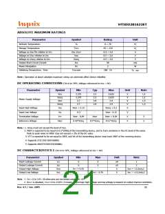
ABSOLUTE MAXIMUM RATINGS
Parameter
Symbol
Rating
Unit
oC
Ambient Temperature
TA
0 ~ 70
oC
V
Storage Temperature
TSTG
VIN, VOUT
VDD
-55 ~ 125
-0.5 ~ 3.6
-0.5 ~ 3.6
-0.5 ~ 3.6
50
Voltage on Any Pin relative to VSS
Voltage on VDD relative to VSS
Voltage on VDDQ relative to VSS
Output Short Circuit Current
Power Dissipation
V
VDDQ
IOS
V
mA
W
PD
2
oC ⋅ sec
Soldering Temperature ⋅ Time
TSOLDER
260 ⋅ 10
Note : Operation at above absolute maximum rating can adversely affect device reliability
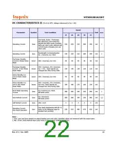
DC OPERATING CONDITIONS (TA=0 to 70oC, Voltage referenced to VSS = 0V)
Parameter
Symbol
Min
Typ
Max
Unit
Note
VDD
VDDQ
VDD
2.375
2.375
2.7
2.5
2.5
2.8
2.8
2.625
2.625
2.9
V
V
V
V
1,4
1,4
1,5
1,5
Power Supply Voltage
VDDQ
2.7
2.9
Input High Voltage
Input Low Voltage
Termination Voltage
Reference Voltage
VIH
VIL
VREF + 0.15
-0.3
-
-
VDDQ + 0.3
VREF - 0.15
VREF + 0.04
0.51*VDDQ
V
V
V
V
VTT
VREF
VREF - 0.04
0.49*VDDQ
VREF
3
2
0.5*VDDQ
Note : 1. VDDQ must not exceed the level of VDD.
2. VREF is expected to be equal to 0.5*VDDQ of the transmitting device, and to track variations in the DC level of the same.
Peak to peak noise on VREF may not exceed ± 2% of the DC value.
3. VTT is expected to be set equal to VREF, and Vtt of the transmitting device must track VREF of the receiving device.
4. Supports 275/ 250/ 200/166Mhz
5. Supports 400/375/350/333/300Mhz
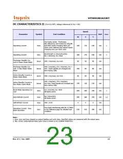
DC CHARACTERISTICS I (TA=0 to 70oC, Voltage referenced to VSS = 0V)
Parameter
Symbol
Min
Max
Unit
Note
Input Leakage Current
Output Leakage Current
Output High Voltage
Output Low Voltage
ILI
ILO
-5
5
uA
uA
V
1
-5
5
2
VOH
VOL
VTT + 0.76
-
-
IOH = -15.2mA,2
IOL = +15.2mA,2
VTT - 0.76
V
Note : 1. VIN = 0 to 3.6V, All other pins are not tested under VIN =0V.
2. DOUT is disabled, VOUT=0 to 2.625V, It means, output logic high voltage and low voltage is depend on output channel conditions.
Rev. 0.5 / Jan. 2005
21

 HYNIX [ HYNIX SEMICONDUCTOR ]