HY2213
1 Cell Li Battery Charge Balance IC
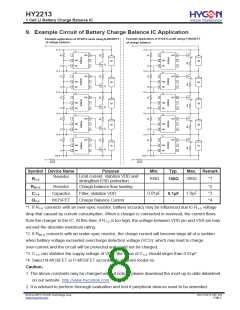
9. Example Circuit of Battery Charge Balance IC Application
Example application of HY2213-xxxB using P-MOSFET
Example application of HY2213-xxxA using N-MOSFET
of charge balance
of charge balance
V5
V5
U5
U5
OUT
OUT
1
2
3
6
5
4
1
2
3
6
5
4
Q5
Q4
Q3
Q2
Q1
VDD
VSS
VDD
VSS
B5
B4
B3
B2
B1
B5
B4
B3
B2
B1
Q5
V4
V4
U4
U4
OUT
OUT
OUT
OUT
OUT
OUT
OUT
OUT
1
2
3
6
5
4
1
2
3
6
5
4
VDD
VSS
VDD
VSS
Q4
V3
V3
U3
U3
1
2
3
6
5
4
1
2
3
6
5
4
VDD
VSS
VDD
VSS
Q3
V2
V2
U2
U2
1
2
3
6
5
4
1
2
3
6
5
4
VDD
VSS
VDD
VSS
Q2
V1
V1
U1
U1
1
2
3
6
5
4
1
2
3
6
5
4
VDD
VSS
VDD
VSS
Q1
VSS
VSS
.
Rsense
Rsense
Symbol Device Name
Purpose
Min.
Typ.
Max. Remark
Limit current, stabilize VDD and
strengthen ESD protection
Resistor
100Ω
200Ω
*1
R1-5
100Ω
Resistor
Capacitor
MOSFET
Charge balance flow loading
Filter, stabilize VDD
*2
*3
*4
RB1-5
C1-5
0.01μF
1.0μF
0.1μF
Charge Balance Control
-
-
-
Q1-5
*1. If R1-5 connects with an over-spec resistor, battery accuracy may be influenced due to R1-5 voltage
drop that caused by current consumption. When a charger is connected in reversed, the current flows
from the charger to the IC. At this time, if R1-5 is too high, the voltage between VDD pin and VSS pin may
exceed the absolute maximum rating.
*2. If RB1-5 connects with an under-spec resistor, the charge current will become large all of a sudden
when battery voltage exceeded overcharge detection voltage (VCU), which may lead to charge
over-current and the circuit will be protected and could not be charged.
*3. C1-5 can stabilize the supply voltage of VDD, the value of C1-5 should larger than 0.01μF.
*4. Select N-MOSFET or P-MOSFET according to different model no.
Caution:
1. The above constants may be changed without notice,please download the most up-to-date datasheet
on our website. http://www.hycontek.com
2. It is advised to perform thorough evaluation and test if peripheral devices need to be amended.
© 2012-2015 HYCON Technology Corp
www.hycontek.com
DS-HY2213-V05_EN
Page 8

 HYCON [ HYCON Technology Corporation ]