HY2213
1 Cell Li Battery Charge Balance IC
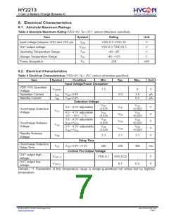
8. Electrical Characteristics
8.1. Absolute Maximum Ratings
Table 4 Absolute Maximum Rating (VSS=0V, Ta=25℃ unless otherwise specified)
Item
Symbol
VDD
Rating
VSS-0.3~VSS+10
VSS-0.3~VDD+0.3
-40~+85
Unit
V
Input voltage between VDD and VSS pin
OUT output voltage
VOUT
TOP
V
Operating Temperature Range
Storage Temperature Range
Power dissipation
℃
TST
-40~+125
℃
PD
250
mW
8.2. Electrical Characteristics
Table 5 Electrical Characteristics (VSS=0V, Ta=25℃ unless otherwise specified)
Item
Symbol
Condition
Min.
Typ.
Max.
Unit
Input Voltage/Power Dissipation
VDD-VSS Operation
Voltage
VDSOP1
-
1.5
-
8
V
Operation Current
Standby Current
IDD
ISB
VDD=3.9V
VDD=2.0V
-
-
2.0
-
3.5
0.5
μA
μA
Detection Voltage
VCU
-0.025
VCU
-0.035
VCR
-0.035
VCR
-0.035
VCU
+0.025
VCU
+0.035
VCR
+0.035
VCR
+0.025
4.0~4.5V adjustable
VCU
VCU
VCR
VCR
2.7
V
V
V
V
V
Overcharge Detection
Voltage
.
VCU
4.0~4.5V adjustable
-5℃~55℃(*1)
3.8~4.5V adjustable
V
CR≠VCU
3.8~4.5V adjustable
CR=VCU
Overcharge Release
Voltage
VCR
VSB
TOC
V
Standby Release
Voltage
2.3
3.1
Delay Time
VDD=3.9V→4.5V
Overcharge Detection
Delay Time
200
250
300
ms
Control Pin Output Voltage
VDD-0.1
OUT output high
voltage
OUT output low
voltage
VOUT_H
VOUT_L
VDD-0.02
0.1
-
V
V
-
0.5
Remark:*1 Parameters of this temperature range is design-guaranteed not actual test by high/low
temperature.
© 2012-2015 HYCON Technology Corp
www.hycontek.com
DS-HY2213-V05_EN
Page 7

 HYCON [ HYCON Technology Corporation ]