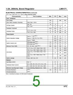
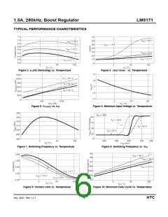
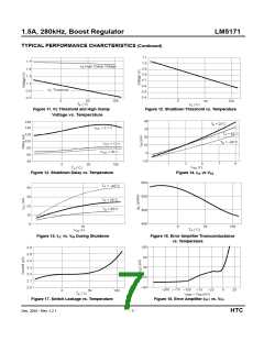
1.5A, 280kHz, Boost Regulator
LM5171
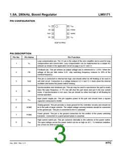
PIN CONFIGURATION
VC
FB
VSW
1
2
3
4
8
7
6
5
PGND
AGND
VCC
Test
SS
SOP-8 PKG
PIN DESCRIPTION
Pin No.
Pin Name
Pin Function
Loop compensation pin. The VC pin is the output of the error amplifier and is used for loop
compensation and current limit. Loop compensation can be implemented by a simple RC
network as shown in the application circuit on page 4 as R1 and C1.
1
VC
FB
Feedback pin. This pin senses an output voltage and is referenced to 1.276V. When the
voltage at this pin falls below 0.4V, chip switching frequency reduces to 20% of the
nominal frequency.
2
3
This pin is connected to internal test logic and should either be left floating or be used in
soft start circuit. Connection to a voltage between 9.5 V and 15 V shuts down the internal
oscillator and leaves the power switch running.
Test
Synchronization and shutdown pin. This pin may be used to synchronize the part to nearly
twice the base frequency. A TTL low will shut the part down and put it into low current
mode. If synchronization is not used, this pin should be either tied high or left floating for
normal operation.
4
SS
Input power supply pin. This pin supplies power to the part and should have a bypass
capacitor connected to AGND.
5
6
7
8
VCC
AGND
PGND
VSW
Analog ground. This pin provides a clean ground for the controller circuitry and should not
be in the path of large currents. The output voltage sensing resistors should be connected
to this ground pin. This pin is connected to the IC substrate.
Power ground. This pin is the ground connection for the emitter of the power switching
transistor. Connection to a good ground plane is essential.
High current switch pin. This pin connects internally to the collector of the power switch.
The open voltage across the power switch can be as high as 40 V. To minimize radiation,
use a trace as short as practical.
Dec. 2010 - Rev. 1.2.1
- 3 -
HTC

 HTC [ HTC KOREA TAEJIN TECHNOLOGY CO. ]