1.5A, 280kHz, Boost Regulator
LM5171
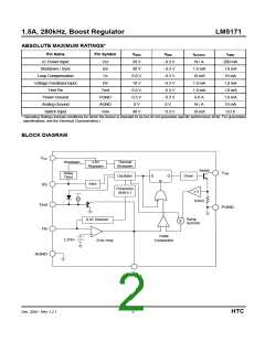
ABSOLUTE MAXIMUM RATINGS*
Pin Name
IC Power Input
Shutdown / Sync
Loop Compensation
Voltage Feedback Input
Test Pin
Pin Symbol
Vcc
VMAX
30 V
30 V
6.0 V
10 V
6.0 V
0.3 V
0 V
VMIN
ISOURCE
N / A
ISINK
- 0.3 V
- 0.3 V
- 0.3 V
- 0.3 V
- 0.3 V
- 0.3 V
0 V
200 mA
1.0 mA
10 mA
1.0 mA
1.0 mA
1.0 mA
10 mA
3.0 A
SS
1.0 mA
10 mA
1.0 mA
1.0 mA
4.0 A
Vc
FB
Test
Power Ground
Analog Ground
Switch Input
PGND
AGND
Vsw
N / A
40 V
- 0.3 V
10 mA
* Operating Ratings indicate conditions for which the device is intended to be but do not guarantee specific performance limits. For guaranteed
specifications, see the Electrical Characteristics.)
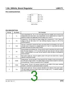
BLOCK DIAGRAM
VCC
Shutdown
2.0V
Thermal
Regulator
Shutdown
Switch
VSW
Delay
Timer
Oscillator
S
Q
Driver
R
Sync
SS
Frequency
Shift 5:1
x 5
63mΩ
Test
PGND
Ramp
Summer
0.4V Detector
+
-
-
FB
+
PWM
1.276V
Error Amp
Comparator
AGND
VC
Dec. 2010 - Rev. 1.2.1
- 2 -
HTC

 HTC [ HTC KOREA TAEJIN TECHNOLOGY CO. ]