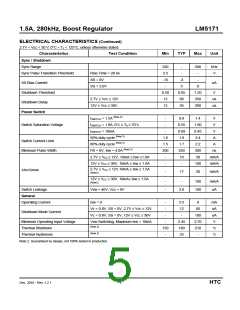
1.5A, 280kHz, Boost Regulator
LM5171
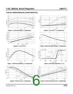
The oscillator is trimmed to guarantee 18% frequency accuracy. The output of the oscillator turns on the
power switch at a frequency of 280 kHz. The power switch is turned off by the output of the PWM Comparator.
A TTL−compatible sync input at the SS pin is capable of syncing up to 1.8 times the base oscillator frequency.
As shown in Figure 20, in order to sync to a higher frequency, a positive transition turns on the power switch
before the output of the oscillator goes high, thereby resetting the oscillator. The sync operation allows multiple
power supplies to operate at the same frequency.
A sustained logic low at the SS pin will shut down the IC and reduce the supply current.
An additional feature includes frequency shift to 20% of the nominal frequency when the FB pin trigger the
threshold. During power up, overload, or short circuit conditions, the minimum switch on−time is limited by the
PWM comparator minimum pulse width. Extra switch off−time reduces the minimum duty cycle to protect
external components and the IC itself.
As previously mentioned, this block also produces a ramp for the slope compensation to improve regulator
stability.
Error Amplifier
VC
LM5171
FB
-
C1
0.01uF
120pF
Voltage
Clamp
1MΩ
+
R1
5kΩ
1.276V
Error Amp
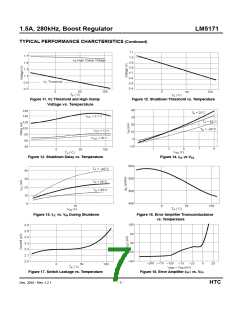
Figure 21. Error Amplifier Equivalent Circuit
The FB pin is directly connected to the inverting input of the positive error amplifier, whose non−inverting input
is fed by the 1.276 V reference. The amplifier is transconductance amplifiers with a high output impedance of
approximately 1 MΩ, as shown in Figure 21. The VC pin is connected to the output of the error amplifiers and
is internally clamped between 0.5 V and 1.7 V. A typical connection at the VC pin includes a capacitor in series
with a resistor to ground, forming a pole/zero for loop compensation.
An external shunt can be connected between the VC pin and ground to reduce its clamp voltage.
Consequently, the current limit of the internal power transistor current is reduced from its nominal value.
Switch Driver and Power Switch
The switch driver receives a control signal from the logic section to drive the output power switch. The
switch is grounded through emitter resistors (63mΩ total) to the PGND pin. PGND is not connected to the IC
substrate so that switching noise can be isolated from the analog ground. The peak switching current is
clamped by an internal circuit. The clamp current is guaranteed to be greater than 1.5A and varies with duty
cycle due to slope compensation. The power switch can withstand a maximum voltage of 40 V on the collector
(VSW pin). The saturation voltage of the switch is typically less than 1V to minimize power dissipation.
Dec. 2010 - Rev. 1.2.1
- 9 -
HTC

 HTC [ HTC KOREA TAEJIN TECHNOLOGY CO. ]