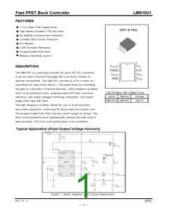
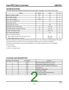
Fast PFET Buck Controller
LM51031
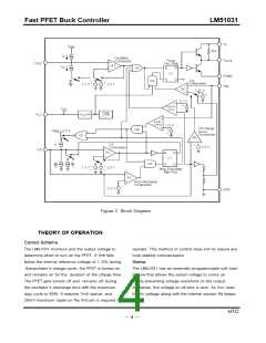
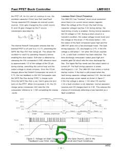
Buck Regulator Operation
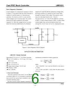
A block diagram of a typical buck regulator is shown
in Figure 4. If we assume that the output transistor is
initially off, and the system is in discontinuous
operation, the inductor current IL is zero and the
output voltage is at its nominal value. The current
drawn by the load is supplied by the output
resistors R1 and R2 and he reference voltage VREF,
the power transistor Q1 switches on and current flows
through the inductor to the output. The inductor current
rises at a rate determined by (VIN − VOUT)/L.
The duty cycle (or “on” time) for the LM51031 is limited
to 80%. If output voltage remains to 80%. If output voltag
remains higher than nominal during the entire COSC
change time, the Q1 does not turn on, skipping the pulse
capacitor CO. When the voltage across CO drops
below the threshold established by the feedback
Figure 4. Buck Regulator Block Diagram
APPLICATIONS INFORMATION
LM51031 Design Example
Specications 12 V to 5.0 V, 3.0 A Buck Controller
Vin = 12 V ±20% (i.e. 14.4 V max, 121 V nom,
9.6 V min)
continuous conduction mode is given by:
Vout = 5.0 V±2%
Iout = 0.3 A to 3.0 A
where:
Output ripple voltage < 50 mV max
Efficiency > 80%
VSAT = RDS(ON) × IOUT max and RDS(ON) is the value at
TJ 100°C.
fSW = 200 kHz
If VF = 0.60 V and VSAT = 0.60 V then the above equati
becomes:
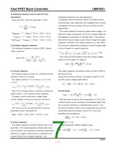
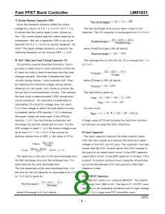
1) Duty Cycle Estimates
Since the maximum duty cycle D, of the LM51031
is limited to 80% min, it is necessary to estimate the
duty cycle for the various input condidtions over the
complete operating range.
The duty cycle for a buck regulator operating in a
HTC
− 6 −

 HTC [ HTC KOREA TAEJIN TECHNOLOGY CO. ]