Fast PFET Buck Controller
LM51031
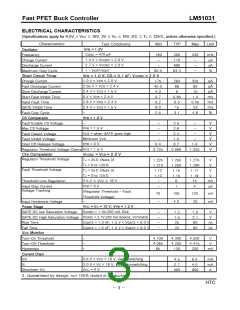
MAXIMUM RATINGS
(Absolute Maximum Ratings indicate limits beyond which damage to the device may occur)
Rating
Symbol
Value
Unit
V
VCC
VC
VGATE
-
Maximum Supply Voltage
Driver Supply Voltage
Driver Output Voltage
COSC, CS, VFB (Logic Pin)
Peak Output Current
20
20
20
V
V
6
V
-
1
A
Steady State Out Current
-
200
mA
℃
℃
℃
kV
TJ
Operating Junction Temperature
Operating Ambient Temperature Range
Storage Temperature Range
0 to 125
0 to 70
-65 to 150
2.0
TA
TS
-
ESD (Human Body Model)
Lead Temperature Soldering
Wave Solder (through hole sytle only) (note 1)
Reflow (SMD styles only) (note 2)
-
-
260 peak
230 peak
℃
℃
Maximum ratings are those value beyond which device damage con occur. Maximum ratings applied to the device
are individual stress limit values (not normal operating conditions) and are not valid simultneously.
If these limits are exceeded, device functional operation is not implied, damage may occur and reliablilty
may be affected.
1. 10 sec. maximum.
2. 60 sec. max above 183℃
PACKAGE LEAD DESCRIPTION
Package Pin Number
Pin Symbol
VGATE
PGND
COSC
GND
Function
Driver pin to gate of external P-ch FET.
Output power stage ground connection.
Oscilator frequency programming capacitor.
Logic ground.
1
2
3
4
5
6
7
8
VFB
Feedback voltage input.
VCC
Logic supply voltage.
CS
Soft-Start and fault timing capacitor.
Driver supply Voltage.
VC
HTC
− 2 −

 HTC [ HTC KOREA TAEJIN TECHNOLOGY CO. ]