Spec. No. : IC200401
Issued Date : 2004.02.01
Revised Date : 2005.07.14
Page No. : 4/8
HI-SINCERITY
MICROELECTRONICS CORP.
Applications Description
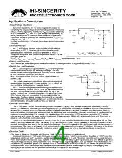
• Output Voltage Adjustment
Like most regulators, H1117 series regulate the output by
comparing the output voltage to an internally generated reference
voltage. On the adjustable version, the VREF is available externally
as 1.25V between VOUT and ADJ. The voltage ratio formed by R1
and R2 should be set to conduct 10mA (minimum output load).
The output voltage is given by the following equation: VOUT =VREF
(1+R2/R1) + IADJ R2
In
Out
VIN
VOUT
ADJ
V REF
R1
R2
IADJ
10uA
On fixed versions of H1117 series, the voltage divider is provided
internally.
• Thermal Protection
H1117 series have thermal protection which limits junction
temperature to 150°C. However, device functionality is only
guaranteed to a maximum junction temperature of +125°C.
The power dissipation and junction temperature for H1117 in all
packages given by
VOUT =VREF (1+R2/R1) + IADJ R2
PD=(VIN - VOUT) IOUT, TJUNCTION=TAMBIENT+(PDxθJA), Note: TJUNCTION must not exceed 125°C
• Current Limit Protection
H1117 series are protected against overload conditions. Current protection is triggered at typically 1.5A.
• Stability And Load Regulation
H1117 series require a capacitor from VOUT to GND to provide
compensation feedback to the internal gain stage. This is to
ensure stability at the output terminal. Typically, a 10uF tantalum
or 50uF aluminum electrolytic is sufficient.
RP
Parasitic
Line Resistance
In
Out
Note : It is important that the ESR for this capacitor does not
exceed 0.5Ω.
The output capacitor does not have a theoretical upper limit
and increasing its value will increase stability. COUT = 100 uF or
more is typical for high current regulator design.
Adj
V IN
R1
Connect
R1 to Case
RL
R2
H1117 series load regulation are limited by the resistance of
the wire connecting it to the load(RP). For the adjustable version,
the best load regulation is accomplished when the top of the
resistor divider(R1) is connected directly to the output pin of the
H1117 series. When so connected, RP is not multiplied by the
divider ratio. For fixed output versions, the top of R1 is internally
connected to the output and ground pin can be connected to low
side of the load as a negative side sense if, so desired.
Connect
R2 to Load
• Thermal Consideration
The H1117 series contain thermal limiting circuitry designed to protect itself for over-temperature conditions. Even for
normal load conditions, maximum junction temperature ratings must not be exceeded. As mention in thermal protection section,
we need to consider all sources of thermal resistance between junction and ambient. It contains junction-to-case, case-to-
heat-sink interface and heat sink resistance itself. An additional heat sink is applied externally sometimes. It can increase the
maximum power dissipation. For example, the equivalent junction temperature of 300mA output current is 115°C without
external heat sink. Under the same junction temperature IC can operates 500mA with an adequate heat sink. Therefore, to
attach an extra heat sink is recommended.
Junction-to-case thermal resistance is specified from the IC junction to the bottom of the case directly below the die. The
bonding wires are appending paths. The former is the lowest resistance path. Proper mounting is required to ensure the best
possible thermal flow this area of the package to the heat sink. Thermal compound at the case-to-heat-sink interface is strongly
recommended. The case of all devices in this series is electrically connected to the output. Therefore, if the case of the device
must be electrically isolated, a thermally conductive spacer can be used, as long its thermal resistance is considered.
• Protection Diode
(The figure is shown as Regulator with Reverse Diode Protection in advanced applications)
In general operation, H1117 series don’t need any protection diodes. From the cross-section structure of H1117 sries, the
output pin is connected to P+ substrate, and the input pin is connected to N- well. There is a parasitic reverse diode between
them. It can handle microsecond surge currents of 5A to 10A. Even with large output capacitance, it is very difficult to get those
values of surge currents in normal operation. Only with high value output capacitors, such as 1000uF. And with the input pin
instantaneously shorted to ground. can damage occur. A crowbar circuit at the input of the H1117 series can generate those
kinds of currents, and a diode from output to input is recommended. Normal power supply cycling or even plugging and
unplugging in the system will not generate currents large enough to do any damage.
H1117 Series
HSMC Product Specification

 HSMC [ HI-SINCERITY MOCROELECTRONICS ]