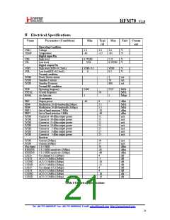
RFM70 V1.0
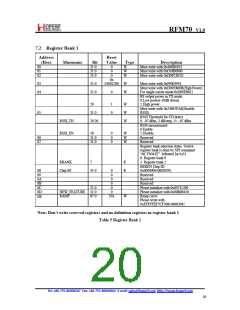
7.2 Register Bank 1
Address
Reset
(Hex)
Mnemonic
Bit
31:0
31:0
31:0
Value
Type
Description
00
01
02
0
W
Must write with 0x404B01E2
Must write with 0xC04B0000
Must write with 0xD0FC8C02
0
0
W
W
0x
03001200
03
04
31:0
31:0
W
W
Must write with 0x99003941
Must write with 0xD99E860B(High Power)
For single carrier mode:0xD99E8621
RF output power in TX mode:
0:Low power(-30dB down)
1:High power
Must write with 0x24067FA6(Disable
RSSI)
RSSI Threshold for CD detect
0: -97 dBm, 2 dB/step, 15: -67 dBm
RSSI measurement:
0
20
1
0
W
W
W
05
31:0
29:26
RSSI_TH
RSSI_EN
0:Enable
1:Disable
Reserved
Reserved
18
31:0
31:0
0
0
0
W
W
W
06
07
Register bank selection states. Switch
register bank is done by SPI command
“ACTIVATE” followed by
0x53
0: Register bank 0
RBANK
Chip ID
7
R
R
1: Register bank 1
BEKEN Chip ID:
0x00000063(RFM70)
Reserved
Reserved
Reserved
Please initialize with 0x00731200
Please initialize with 0x0080B436
Ramp curve
08
09
31:0
0
0
0
0
0
0A
0B
0C
0D
0E
31:0
NEW_FEATURE 31:0
RAMP 87:0
0
NA
W
Please write with
0xFFFFFEF7CF208104082041
Note: Don’t write reserved registers and no definition registers in register bank 1
Table 5 Register Bank 1
Tel: +86‐755‐86096587 Fax: +86‐755‐86096602 E‐mail: sales@hoperf.com http://www.hoperf.com
20

 HOPERF [ HOPERF ]