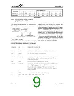
HT46R01A
Absolute Maximum Ratings
Supply Voltage...........................VSS-0.3V to VSS+6.0V
Input Voltage..............................VSS-0.3V to VDD+0.3V
IOL Total ..............................................................150mA
Total Power Dissipation .....................................500mW
Storage Temperature............................-50°C to 125°C
Operating Temperature...........................-40°C to 85°C
IOH Total............................................................-100mA
Note: These are stress ratings only. Stresses exceeding the range specified under ²Absolute Maximum Ratings² may
cause substantial damage to the device. Functional operation of this device at other conditions beyond those listed
in the specification is not implied and prolonged exposure to extreme conditions may affect device reliability.
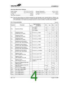
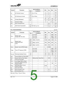
D.C. Characteristics
Ta=25°C
Test Conditions
Conditions
Symbol
Parameter
Min.
Typ.
Max.
Unit
VDD
¾
f
SYS=4MHz
2.2
3.3
4.5
¾
5.5
5.5
5.5
2
V
¾
¾
¾
1
VDD
fSYS=8MHz
SYS=12MHz
Operating Voltage
V
¾
f
V
¾
3V
5V
3V
5V
mA
mA
mA
mA
Operating Current
IDD1
No load, fSYS=4MHz
(Crystal OSC, RC OSC)
2.5
2
5
¾
4
¾
Operating Current
IDD2
IDD3
IDD4
No load, fSYS=8MHz
No load, fSYS=12MHz
No load, fSYS=4MHz
(Crystal OSC, RC OSC)
4
8
¾
Operating Current
5V
6
12
mA
¾
(Crystal OSC, RC OSC)
3V
5V
3V
5V
1
2.5
2
2
5
4
8
mA
mA
mA
mA
¾
¾
¾
¾
Operating Current (Internal
RC+RTC OSC, Normal Mode)
Operating Current (Internal
IDD5
IDD6
IDD7
No load, fSYS=8MHz
No load, fSYS=12MHz
No load, fSYS=32768Hz
RC+RTC OSC, Normal Mode)
4
Operating Current (Internal
5V
6
12
mA
¾
RC+RTC OSC, Normal Mode)
3V
5V
3V
5V
3V
5V
3V
5V
20
40
¾
¾
¾
¾
¾
¾
30
60
5
¾
¾
¾
¾
¾
¾
¾
¾
mA
mA
mA
mA
mA
mA
mA
mA
Operating Current (Internal
RC+RTC OSC, Slow Mode)
Standby Current
ISTB1
ISTB2
ISTB3
No load, system HALT
No load, system HALT
(WDT Enabled, RTC Off)
10
1
Standby Current
(WDT Disabled, RTC Off)
2
5
Standby Current
No load, system HALT
QOSC=1
(WDT Disabled, RTC On)
10
Input Low Voltage for PA0~PA7,
TMR0 and INT
VIL1
0.3VDD
VDD
0
V
V
¾
¾
¾
¾
¾
¾
Input High Voltage forPA0~PA7,
TMR0 and INT
VIH1
0.7VDD
VIL2
0.4VDD
VDD
Input Low Voltage (RES)
Input High Voltage (RES)
Low Voltage Reset 1
Low Voltage Reset 2
Low Voltage Reset 3
0
V
V
V
V
V
¾
¾
¾
¾
¾
¾
¾
¾
VIH2
0.9VDD
3.98
¾
VLVR1
VLVR2
VLVR3
Configuration option: 4.2V
Configuration option: 3.15V
Configuration option: 2.1V
4.2
3.15
2.1
4.42
2.98
3.32
1.98
2.22
Rev. 1.10
4
August 13, 2008

 HOLTIC [ HOLT INTEGRATED CIRCUITS ]