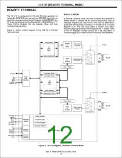
HI-6110 (REMOTE TERMINAL MODE)
REGISTER FORMATS (RT Mode)
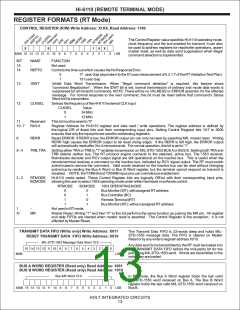
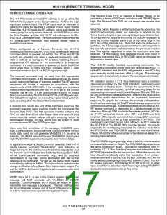
CONTROL REGISTER (R/W) Write Address: X1XX, Read Address: 1100
The Control Register value specifies HI-6110 operating mode,
IDWT
clock frequency and the bus enabled for transmit. It can also
be used to address registers for read/write operations, assert
master reset, as well as data word suppression when illegal
command detection is implemented .
X
0
1
0
X
MSB 15 14 13 12 11 10
9
8
7
6
5
4
3
2
1
0
LSB
BIT
15
NAME
-
FUNCTION
Not used.
14
REPTO
Controls the time-out which causes the No Response Error.
0
1
17 usec Gap (equivalent to the 57 usec measurement of 5.2.1.7 of the RTValidation Test Plan)
131 usec Gap
13
12
IDWT
Inhibit Data Word Transmission. When “illegal command detection” is required, this feature alows
“command illegalization”. When the IDWT bit is set, normal transmission of ordinary and mode data words is
suppressed for all transmit commands. NOTE: There will be no VALMESS or ERROR assertion for the affected
message. For normal response to the next command, this bit must be reset before that command’s Status
Word bit 0 is transmitted.
CLKSEL
Selects the frequency of the HI-6110 external CLK input:
CLKSEL
Value
24 MHz
12 MHz
0
1
11
Reserved
RA3:0
This bit must be reset to “0”
10 - 7
Register Address for HI-6110 register and data read / write operations. The register address is defined by
the logical OR of these bits and their corresponding input pins. Setting Control Register bits 10:7 to 0000
ensures that only the input pins are used for addressing registers.
6
RERR
Reset ERROR. If RERR is low, the ERROR output pin can only be reset by asserting MR, master reset. Writing
RERR high causes the ERROR output to be reset (rising edge). If the RERR is left high, the ERROR output
will automatically reset after 3 to 4 microseconds. For normal operation, this bit is set to “1”.
5 - 4
TRB, TRA
Setting either TRA or TRB to "1" enables transmission on MIL-STD-1553 BUS A or BUS B. Setting both TRA and
TRB selects neither bus. The RT protocol engine connects to the selected, active bus. The 1553 receiver,
Manchester decoder and RCV output signal are still operational on the inactive bus. This is useful when the
remote terminal receives a command on the inactive bus, indicated by RCV signal output. The RT must switch
active buses to service the command. Valid words received on the inactive bus can be read without changing
active bus by reading the Bus A Word or Bus B Word register, but the terminal cannot respond as transmit is
disabled. NOTE: theTXINHAandTXINHB input pins can override bus enablement.
3 - 2
RTMODE, HI-6110 mode select. These Control Register bits are logically OR'ed with their corresponding input pins,
allowing the user to select 1553 operating mode under either hardware or software control:
BCMODE
RTMODE
BCMODE
1553 OPERATING MODE
0
0
1
1
0
1
0
1
Bus Monitor (MT), with assigned RTaddress
Bus Controller (BC)
RemoteTerminal (RT)
Bus Monitor (MT), without assigned RTaddress
1
-
Not used in RTmode.
!0
MR
Master Reset. Writing "1" and then “0” to this bit performs the same function as pulsing the MR pin. All register
and data FIFOs are cleared when master reset is asserted. The Control Register is the exception; it is not
affected by Master Reset.
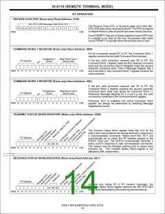
TRANSMIT DATA FIFO (Write only) Write Address: X011
RESET TRANSMIT DATA FIFO Write Address: X010
The Transmit Data FIFO is 32-words deep and holds MIL-
STD-1553 message data. The FIFO is cleared on Master
Reset or by any write to register address X010.
MIL-STD-1553 Message Data Word 15:0
Any data word to be transmitted by the RT must be loaded into
the TRANSMIT DATA FIFO before the mid-parity bit for the
preceding MIL-STD-1553 word. Words are transmitted in the
order they are loaded.
15 14 13 12 11 10
9
8
7
6
5
4
3
2
1
0
MSB
LSB
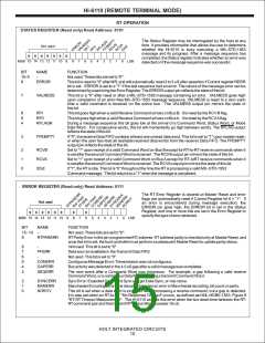
BUS A WORD REGISTER (Read only) Read Address: 1001
BUS B WORD REGISTER (Read only) Read Address: 1010
Bus A/B Word 15:0
In RT mode, the Bus A Word register holds the last valid
MIL-STD-1553 word received on Bus A. The Bus B Word
register holds the last valid MIL-STD-1553 word received on
Bus B.
MSB 15 14 13 12 11 10
9
8
7
6
5
4
3
2
1
0
LSB
HOLT INTEGRATED CIRCUITS
13

 HOLTIC [ HOLT INTEGRATED CIRCUITS ]