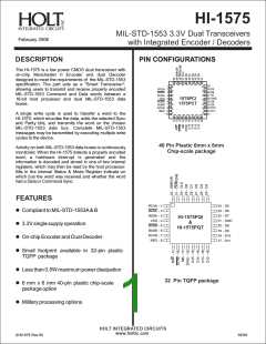
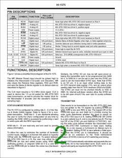
HI-1575
PIN DESCRIPTIONS
PULL-UP
PULL-DOWN
PIN
(TQFP)
SYMBOL FUNCTION
DESCRIPTION
1
2
RCVA
BUSA
BUSA
VDD
Digital output
Analog I/O
-
-
-
-
-
-
-
Goes high when MIL-STD-1553 word received on Bus A
MIL-STD-1533 bus driver A, negative signal
MIL-STD-1553 bus driver A, positive signal
+3.3 VDCr
3
Analog I/O
4
Power supply
Analog I/O
5,
6
BUSB
BUSB
RCVB
REG
MIL-STD-1533 bus driver B, negative signal
MIL-STD-1553 bus driver B, positive signal
Goes high when MIL-STD-1553 word received on Bus B
Analog I/O
7
Digital output
8
Digital input 12K pull-down Selects Status & Mode Register when high, or Data registers when low
9
R/W
Digital input
Digital input
12K pull-up
12K pull-up
Controls data and sync direction during read or write operations
Strobe. Timing input to control register read and write operations
10
11
12
STRB
MR
Digital input 12K pull-down Pulse high to reset the HI-1575
SYNC
Digital I/O
Digital I/O
12K pull-down Selects transmit sync type on write, indicates received sync type on read.
12K pull-down Data bus. D15 (MSB) corresponds to MIL-STD-1553 bit 4
13-20, 22-29 D15:D0
21
30
31
32
GND
CLK
Power supply
Digital input
-
-
Ground
12 MHz clock
CHA/CHB Digital Input 12K pull-down Selects MIL-STD-1553 Bus A or Bus B
ERROR Digital output
-
Goes high when a received MIL-STD-1553 word has an encoding error
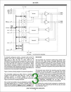
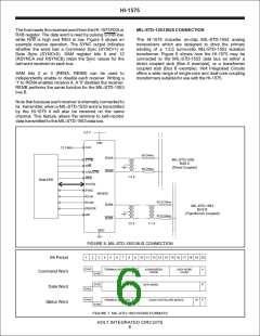
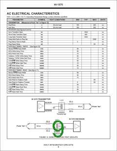
FUNCTIONAL DESCRIPTION
Figure 1 shows a simplified block diagram of the HI-1575.
Similarly, the SYNC I/O pin may be left open-circuit al-
lowing the transmitter sync to be programmed into SAM
The MR (Master Reset) input should be pulsed high to
initialize the Manchester II Encoder and Decoders. MR
also clears the Receive Data registers, RXA and RXB,
and sets the Status & Mode register to its default state as
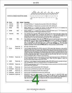
described in figure 2.
bit 4, or SAM bit 4 can be set to zero and the SYNC pin
used to set the transmitted SYNC type. Note that SYNC
is an I/O pin. It is an input when writing data to the
HI-1575 transmit data register (TX), and an output when
reading data from the HI-1575 receivers (RXA and RXB).
The SYNC pin must not be shorted directly to VDD or
GND. An internal pull-down resistor allow the SYNC pin
to be left open-circuit if the user opts for purely software
control.
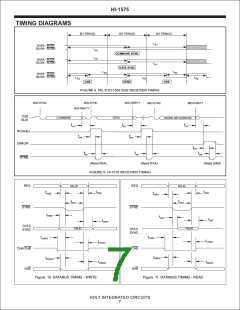
The CLK input requires a 12.0 MHz clock signal. CLK is
used to derive the 1.0 us bit period for MIL-STD-1553
data transmission, as well to provide the master clock for
the Manchester II encoder and the decoder's receiver
sampling logic.
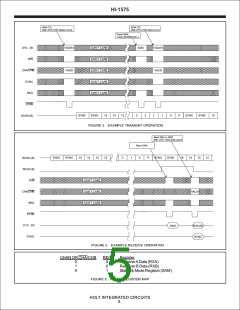
TRANSMITTER
STATUS & MODE REGISTER
Data words to be transmitted on the MIL-STD-1553 data
bus are written to the TX register by pulsing STRB low
while R/W is low and REG is low. The logical OR of the
CHA/CHB input pin and SAM bit 5 (CHAN) during the
write cycle determines whether the word is output on
MIL-STD-1553 bus A or B. Setting CHA/CHB OR CHAN
to a zero selects bus A, and a one selects bus B. The log-
ical OR of the SYNC pin and SAM bit 4 (TXSYNC) dur-
ing the write cycle defines whether the transmitted word
is a MIL-STD-1553 Command or Data word. Setting
SYNC to a one causes a Command (or Status) sync to
be generated. Setting SYNC to zero selects a Data sync.
Note that the SYNC pin is bidirectional. It should be
treated as an extension to the 16-bit bidirectional
databus (D15:D0) in terms of I/O switching and timing.
The HI-1575 is configured by writing bits 0 - 5 of the Sta-
tus & Mode (SAM) register. Refer to figure 2 for a com-
plete description. SAM bits 0 - 5 are read/write allowing
the user to verify the chip's configuration at any time by
reading the SAM. SAM is accessed by performing a read
or write cycle with the REG input high.
SAM bits 6 - 15 are read-only and are used to provide
status information.
To allow the user to minimize the number of hardware
control inputs, SAM bit 5 (Channel A/B select) is logically
'OR'ed with the CHA/CHB input pin. To select between
MIL-STD-1553 bus A or B, the user may either tie the
CHA/CHB pin low and select buses using SAM bit 5
(software control), or program SAM bit 5 to a zero and
use the CHA/CHB pin to select the active bus (hardware
control).
The HI-1575 automatically calculates and appends the cor-
rect parity bit to the transmitted word. Each word is as-
signed odd parity as required by MIL-STD-1553.
HOLT INTEGRATED CIRCUITS
2

 HOLTIC [ HOLT INTEGRATED CIRCUITS ]