HT46R01B/02B/01N/02N
HT48R01B/02B/01N/02N
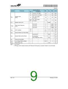
Note: I/T: Input type
O/T: Output type
OPT: Optional by configuration option (CO) or register option
PWR: Power
CO: Configuration option
ST: Schmitt Trigger input
CMOS: CMOS output
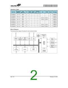
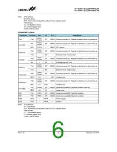
The important point to note here is that the PB0 and PB1 pads will not be bounded to pins in the 10-pin MSOP
package. These two pads default to an input state, the designer should set the register PBPU to pull high op-
tions. In this way, these two internal pads can be pulled up in order to prevent input pin floating power con-
sumption.
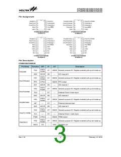
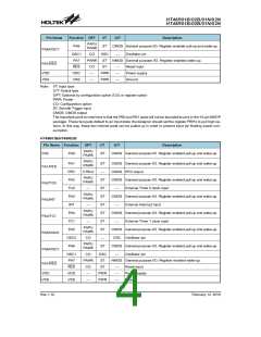
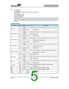
HT46R01N/HT46R02N
Pin Name
Function OPT
I/T
ST
AN
ST
O/T
CMOS General purpose I/O. Register enabled pull-up and wake-up.
A/D channel 0
Description
PAPU
PA0
PAWK
PA0/AN0
AN0
PA1
ADCR
¾
PAPU
PAWK
CMOS General purpose I/O. Register enabled pull-up and wake-up.
CMOS PFD output
PA1/PFD/AN1
PA2/TC0/AN2
PA3/INT/AN3
PFD
AN1
CTRL0
ADCR
¾
AN
A/D channel 1
CMOS General purpose I/O. Register enabled pull-up and wake-up.
¾
PAPU
PAWK
PA2
ST
TC0
AN2
ST
AN
External Timer 0 clock input
A/D channel 2
¾
¾
¾
ADCR
PAPU
PAWK
PA3
ST
CMOS General purpose I/O. Register enabled pull-up and wake-up.
INT
ST
AN
External interrupt input
A/D channel 3
¾
¾
¾
AN3
ADCR
PAPU
PAWK
PA4
ST
CMOS General purpose I/O. Register enabled pull-up and wake-up.
External Timer 1 clock input
PA4/TC1/PWM
PA5/OSC2
TC1
ST
¾
¾
PWM
CTRL0
CMOS PWM output
¾
PAPU
PAWK
PA5
OSC2
PA6
ST
¾
CMOS General purpose I/O. Register enabled pull-up and wake-up.
OSC Oscillator pin
CO
PAPU
PAWK
ST
CMOS General purpose I/O. Register enabled pull-up and wake-up.
PA6/OSC1
PA7/RES
OSC1
PA7
CO
PAWK
CO
OSC
ST
Oscillator pin
NMOS General purpose I/O. Register enabled wake-up.
Reset input
¾
RES
PB0
ST
¾
PB0
PB1
VDD
VSS
PBPU
PBPU
¾
ST
CMOS General purpose I/O. Register enabled.
CMOS General purpose I/O. Register enabled.
PB1
ST
VDD
VSS
PWR
PWR
Power supply
Ground
¾
¾
¾
Rev.1.10
5
February 12, 2010

 HOLTEK [ HOLTEK SEMICONDUCTOR INC ]