HT46R01B/02B/01N/02N
HT48R01B/02B/01N/02N
T
i
m
e
r
O
v
e
r
f
l
o
w
P
F
D
C
l
o
c
k
P
A
1
D
a
t
a
P
F
D
O
u
t
p
u
t
a
t
P
A
1
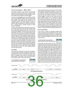
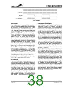
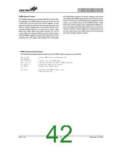
PFD Function
PFD Function
Programming Considerations
The Programmable Frequency Divider provides a
means of producing a variable frequency output suitable
for applications, such as piezo-buzzer driving or other
interfaces requiring a precise frequency generator.
When configured to run in the timer mode, the internal
system clock is used as the timer clock source and is
therefore synchronised with the overall operation of the
microcontroller. In this mode when the appropriate timer
register is full, the microcontroller will generate an internal
interrupt signal directing the program flow to the respec-
tive internal interrupt vector. For the pulse width capture
mode, the internal system clock is also used as the timer
clock source but the timer will only run when the correct
logic condition appears on the external timer input pin. As
this is an external event and not synchronised with the in-
ternal timer clock, the microcontroller will only see this ex-
ternal event when the next timer clock pulse arrives. As a
result, there may be small differences in measured val-
ues requiring programmers to take this into account dur-
ing programming. The same applies if the timer is
configured to be in the event counting mode, which again
is an external event and not synchronised with the inter-
nal system or timer clock.
The Timer/Event Counter overflow signal is the clock
source for the PFD function, which is controlled by
PFDCS bit in CTRL0. For applicable devices the clock
source can come from either Timer/Event Counter 0 or
Timer/Event Counter 1. The output frequency is con-
trolled by loading the required values into the timer
prescaler and timer registers to give the required division
ratio. The counter will begin to count-up from this preload
register value until full, at which point an overflow signal is
generated, causing both the PFD outputs to change
state. The counter will then be automatically reloaded
with the preload register value and continue counting-up.
If the CTRL0 register has selected the PFD function,
then for PFD output to operate, it is essential for the Port
Acontrol register PAC, to setup the PFD pins as outputs.
PA1 must be set high to activate the PFD. The output
data bits can be used as the on/off control bit for the PFD
outputs. Note that the PFD outputs will all be low if the
output data bit is cleared to zero.
When the Timer/Event Counter is read, or if data is writ-
ten to the preload register, the clock is inhibited to avoid
errors, however as this may result in a counting error, this
should be taken into account by the programmer. Care
must be taken to ensure that the timers are properly in-
itialised before using them for the first time. The associ-
ated timer enable bits in the interrupt control register must
be properly set otherwise the internal interrupt associated
with the timer will remain inactive. The edge select, timer
mode and clock source control bits in timer control regis-
ter must also be correctly set to ensure the timer is prop-
erly configured for the required application. It is also
important to ensure that an initial value is first loaded into
the timer registers before the timer is switched on; this is
because after power-on the initial values of the timer reg-
isters are unknown. After the timer has been initialised
the timer can be turned on and off by controlling the en-
able bit in the timer control register.
Using this method of frequency generation, and if a
crystal oscillator is used for the system clock, very pre-
cise values of frequency can be generated.
I/O Interfacing
The Timer/Event Counter, when configured to run in the
event counter or pulse width capture mode, requires the
use of an external timer pin for its operation. As this pin is
a shared pin it must be configured correctly to ensure that
it is setup for use as a Timer/Event Counter input pin. This
is achieved by ensuring that the mode select bits in the
Timer/Event Counter control register, select either the
event counter or pulse width capture mode. Additionally
the corresponding Port Control Register bit must be set
high to ensure that the pin is setup as an input. Any
pull-high resistor connected to this pin will remain valid
even if the pin is used as a Timer/Event Counter input.
Rev.1.10
38
February 12, 2010

 HOLTEK [ HOLTEK SEMICONDUCTOR INC ]