HT46R064G/065G/0662G
Enhanced A/D Type 8-Bit OTP MCU with OPA
Summary of A/D Conversion Steps
The following summarises the individual steps that should be executed in order to implement an A/D
conversion process.
Step 1
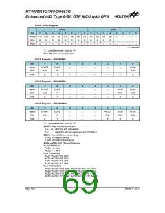
Select the required A/D conversion clock by correctly programming bits ADCS2, ADCS1 and
ADCS0 in the register.
Step 2
Select which pins are to be used as A/D inputs and configure them as A/D input pins by correctly
programming the PCR7~PCR0 bits in the ANCSR or PCR register.
Step 3
Enable the A/D converter by clearing the ADONB bit in the ACSR register zero.
Step 4
Select which channel is to be connected to the internal A/D converter by correctly programming the
ACS2~ACS0 bits which are also contained in the register.
Step 5
If the interrupts are to be used, the interrupt control registers must be correctly configured to ensure the
A/D converter interrupt function is active. The master interrupt control bit, EMI, the INTC0 interrupt
control register must be set to 1, the A/D converter interrupt bit, ADE, in the INTC1 register must also
be set to 1.
Step 6
The analog to digital conversion process can now be initialised by setting the START bit in the ADCR
register from 0 to 1 and then to 0 again. Note that this bit should have been originally set to 0.
Step 7
To check when the analog to digital conversion process is complete, the EOCB bit in the ADCR
register can be polled. The conversion process is complete when this bit goes low. When this occurs,
the A/D data registers ADRL and ADRH can be read to obtain the conversion value. As an alternative
method if the interrupts are enabled and the stack is not full, the program can wait for an A/D interrupt
to occur.
Note: When checking for the end of the conversion process, if the method of polling the EOCB bit in the
ADCR register is used, the interrupt enable step above can be omitted.
The accompanying diagram shows graphically the various stages involved in an analog to digital
conversion process and its associated timing.
The setting up and operation of the A/D converter function is fully under the control of the applica-
tion program as there are no configuration options associated with the A/D converter. After an A/D
conversion process has been initiated by the application program, the microcontroller internal hard-
ware will begin to carry out the conversion, during which time the program can continue with other
functions. The time taken for the A/D conversion is 16 tAD clock cycles where tAD is equal to the A/D
clock period.
Rev. 1.00
73
March 3, 2011

 HOLTEK [ HOLTEK SEMICONDUCTOR INC ]