HT46F46E/HT46F47E/HT46F48E/HT46F49E
b
7
b
0
P
W
M
,
P
W
M
0
,
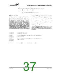
P
W
M
1
R
e
g
i
s
t
e
r
s
A
D
C
v
a
l
u
u
e
C
v
a
l
e
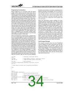
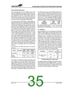
7+1 Mode Pulse Width Modulation Register
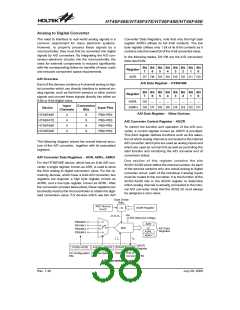
PWM Output Control
disable the PWM output function and force the output
low. In this way, the Port D data output register can be
used as an on/off control for the PWM function. Note
that if the configuration options have selected the PWM
function, but a ²1² has been written to its corresponding
bit in the PDC control register to configure the pin as an
input, then the pin can still function as a normal input
line, with pull-high resistor options.
On all devices, the PWM outputs are pin-shared with
pins PD0 or PD1. To operate as PWM outputs and not
as I/O pins, the correct PWM configuration options must
be selected. A ²0² must also be written to the corre-
sponding bits in the I/O port control register PDC to en-
sure that the required PWM output pin is setup as an
output. After these two initial steps have been carried
out, and of course after the required PWM value has
been written into the PWM register, writing a ²1² to the
corresponding bit in the PD output data register will en-
able the PWM data to appear on the pin. Writing a ²0² to
the corresponding bit in the PD output data register will
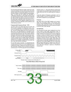
PWM Programming Example
The following sample program shows how the PWM
outputs are setup and controlled. Before use the corre-
sponding PWM output configuration options must first
be selected.
clr PDC.0
clr PDC.1
; set pin PD0 as output
; set pin PD1 as output
set pd.0
mov a,64h
mov pwm0,a
; PD.0=1; enable pin ²PD0/PWM0² to be the PWM channel 0
; PWM0=100D=64H
set pd.1
mov a,65h
mov pwm1,a
; PD.1=1; enable pin ²PD1/PWM1² to be the PWM channel 1
; PWM1=101D=65H
clr pd.0
clr pd.1
; disable PWM0 output - PD.0 will remain low
; disable PWM1 output - PD.1 will remain low
Rev. 1.40
37
July 28, 2009

 HOLTEK [ HOLTEK SEMICONDUCTOR INC ]