HT46F46E/HT46F47E/HT46F48E/HT46F49E
Pulse Width Modulator
Each microcontroller in the Cost-Effective A/D Flash
Type with EEPROM MCU series contains either one or
two Pulse Width Modulation (PWM) outputs. Useful for
such applications such as motor speed control, the
PWM function provides outputs with a fixed frequency
but with a duty cycle that can be varied by setting partic-
ular values into the corresponding PWM register.
the PWM cycle frequency and the PWM modulation fre-
quency should be understood. As the PWM clock is the
system clock, fSYS, and as the PWM value is 8-bits wide,
the overall PWM cycle frequency is fSYS/256. However,
when in the 7+1 mode of operation the PWM modulation
frequency will be fSYS/128, while the PWM modulation
frequency for the 6+2 mode of operation will be fSYS/64.
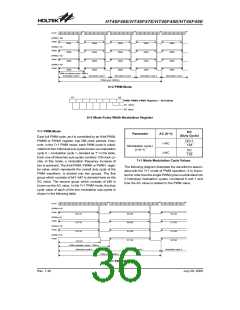
For devices with one PWM output, a single register, lo-
cated in the Data Memory is assigned to the Pulse Width
Modulator and is known as the PWM register. For de-
vices with two PWM outputs, two registers are provided
and are known as PWM0 and PWM1. It is here that the
8-bit value, which represents the overall duty cycle of
one modulation cycle of the output waveform, should be
placed. To increase the PWM modulation frequency,
each modulation cycle is subdivided into two or four indi-
vidual modulation subsections, known as the 7+1 mode
or 6+2 mode respectively. Each device can choose
which mode to use by selecting the appropriate configu-
ration option. When a mode configuration option is cho-
sen, it applies to all PWM outputs on that device. Note
that when using the PWM, it is only necessary to write
the required value into the appropriate PWM register
and select the required mode configuration option, the
subdivision of the waveform into its sub-modulation cy-
cles is done automatically within the microcontroller
hardware.
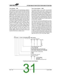
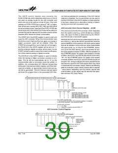
PWM
PWM
Cycle
PWM
Cycle
Duty
Modulation
Frequency
Frequency
f
f
SYS/64 for (6+2) bits mode
SYS/128 for (7+1) bits mode
f
SYS/256
[PWM]/256
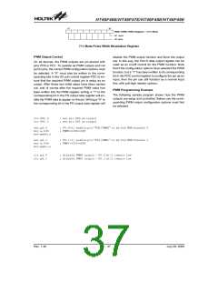
6+2 PWM Mode
Each full PWM cycle, as it is controlled by an 8-bit PWM,
PWM0 or PWM1 register, has 256 clock periods. How-
ever, in the 6+2 PWM mode, each PWM cycle is subdi-
vided into four individual sub-cycles known as
modulation cycle 0 ~ modulation cycle 3, denoted as i in
the table. Each one of these four sub-cycles contains 64
clock cycles. In this mode, a modulation frequency in-
crease of four is achieved. The 8-bit PWM, PWM0 or
PWM1 register value, which represents the overall duty
cycle of the PWM waveform, is divided into two groups.
The first group which consists of bit2~bit7 is denoted
here as the DC value. The second group which consists
of bit0~bit1 is known as the AC value. In the 6+2 PWM
mode, the duty cycle value of each of the four modula-
tion sub-cycles is shown in the following table.
For all devices, the PWM clock source is the system
clock fSYS
.
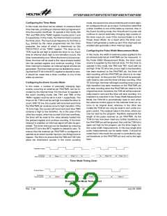
PWM Output Register
Device
Channels
DC
Mode
Pins
Name
Parameter
AC (0~3)
i<AC
(Duty Cycle)
6+2 or PD0/
PWM0/
PWM1
HT46F49E
2
1
DC+1
7+1
PD1
PD0
64
Modulation cycle i
(i=0~3)
Other
6+2 or
7+1
PWM
DC
64
Devices
i³AC
6+2 Mode Modulation Cycle Values
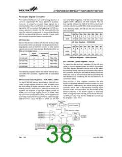
This method of dividing the original modulation cycle
into a further 2 or 4 sub-cycles enable the generation of
higher PWM frequencies which allow a wider range of
applications to be served. As long as the periods of the
generated PWM pulses are less than the time constants
of the load, the PWM output will be suitable as such long
time constant loads will average out the pulses of the
PWM output. The difference between what is known as
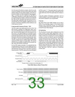
The following diagram illustrates the waveforms associ-
ated with the 6+2 mode of PWM operation. It is impor-
tant to note how the single PWM cycle is subdivided into
4 individual modulation cycles, numbered from 0~3 and
how the AC value is related to the PWM value.
Rev. 1.40
35
July 28, 2009

 HOLTEK [ HOLTEK SEMICONDUCTOR INC ]