HT46F46E/HT46F47E/HT46F48E/HT46F49E
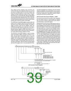
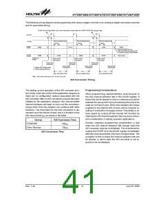
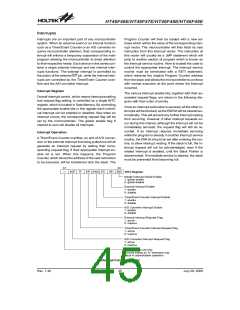
The following timing diagram shows graphically the various stages involved in an analog to digital conversion process
and its associated timing.
S
T
A
R
T
b
i
t
s
e
t
h
i
g
h
w
i
t
h
i
n
o
n
e
t
o
t
e
n
i
n
s
t
r
u
c
t
i
o
n
c
y
c
l
e
S
T
A
R
T
A
/
D
s
a
m
p
l
i
n
g
A
/
t
D
i
m
s
e
a
m
p
l
i
n
g
A
/
t
D
i
m
s
e
a
m
p
l
i
n
g
t
i
m
e
E
O
C
B
A
3
D
2
t
A
3
D
2
t
A
3
D
2
t
P
C
R
2
~
0
0
0
B
0
1
1
B
1
0
0
B
0
0
0
B
P
C
R
0
1
.
P
B
p
o
r
t
s
e
2
.
A
/
D
c
o
n
v
e
t
o
r
e
d
u
c
e
A
C
S
2
~
0
0
0
B
0
1
0
B
0
0
0
B
0
0
1
B
D
o
n
'
t
c
a
r
e
A
C
S
0
P
o
w
e
r
-
o
n
S
c
t
a
r
t
o
f
A
/
D
S
t
a
r
t
o
f
A
/
D
S
t
a
r
t
o
f
A
/
D
R
e
s
e
t
o
n
v
e
r
s
i
o
n
c
o
n
v
e
r
s
i
o
n
c
o
n
v
e
r
s
i
o
n
R
e
s
e
t
A
/
D
R
e
s
e
t
A
/
D
R
e
s
e
t
A
/
D
c
o
n
v
e
r
t
e
r
c
o
n
v
e
r
t
e
r
c
o
n
v
e
r
t
e
r
E
n
d
o
f
A
/
D
E
n
d
o
f
A
/
D
E
n
d
o
f
A
/
D
c
o
n
v
e
r
s
i
o
n
n
c
o
n
v
e
r
s
i
o
n
c
o
n
v
e
r
s
i
o
n
1
:
D
e
f
i
n
e
P
B
c
o
n
f
i
g
u
r
a
t
i
o
2
:
S
e
l
e
c
t
a
n
a
l
o
g
c
h
a
n
n
e
l
t
A
D
C
t
A
D
C
t
A
D
C
A
/
D
c
o
n
v
e
r
s
i
A
o
/
n
D
t
c
i
m
o
n
e
v
e
r
s
i
A
o
/
n
D
t
c
i
m
o
n
e
v
e
r
s
i
o
n
t
i
m
e
N
o
t
A
e
/
:
D
c
l
o
S
c
Y
/
k
S
2
S
,
m
Y
/
S
u
8
f
s
S
o
Y
t
/
S
r
3
b
2
f
e
f
A/D Conversion Timing
Programming Considerations
The setting up and operation of the A/D converter func-
tion is fully under the control of the application program as
there are no configuration options associated with the
A/D converter. After an A/D conversion process has been
initiated by the application program, the microcontroller
internal hardware will begin to carry out the conversion,
during which time the program can continue with other
functions. The time taken for the A/D conversion is de-
pendent upon the device chosen and is a function of the
A/D clock period tAD as shown in the table.
When programming, special attention must be given to
the A/D channel selection bits in the ADCR register. If
these bits are all cleared to zero no external pins will be
selected for use as A/D input pins allowing the pins to be
used as normal I/O pins. When this happens the power
supplied to the internal A/D circuitry will be reduced re-
sulting in a reduction of supply current. This ability to re-
duce power by turning off the internal A/D function by
clearing the A/D channel selection bits may be an impor-
tant consideration in battery powered applications.
Device
HT46F46E
Other Devices
A/D Conversion Time
Another important programming consideration is that
when the A/D channel selection bits change value the
A/D converter must be re-initialised. This is achieved by
pulsing the START bit in the ADCR register immediately
after the channel selection bits have changed state. The
exception to this is where the channel selection bits are
all cleared, in which case the A/D converter is not re-
quired to be re-initialised.
64tAD
76tAD
A/D Conversion Time
Rev. 1.40
41
July 28, 2009

 HOLTEK [ HOLTEK SEMICONDUCTOR INC ]