HT46R63/HT46C63
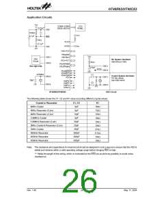
Application Circuits
V
D
D
C
O
M
0
~
C
O
M
3
L
C
D
m
0 . 0 1 F *
S
E
G
0
~
S
E
G
1
8
P
A
N
E
L
V
R
D
D
S
1
0
0
k
V
D
D
m
0 . 1 F
E
1
0
k
V
L
C
D
m
0 . 1 F *
A
V
D
D
V
D D
V
S
S
P
A
0
~
P
A
7
P
B
0
/
A
N
0
7
V
D
D
O
O
S
S
C
C
1
2
P
B
7
/
A
N
O
S
C
R
C
S
y
s
t
e
m
O
s
c
i
l
l
a
t
o
r
P
C
0
~
P
C
7
C
i
r
c
u
i
t
2
4
k
W
O
S
C
W
R
O
S
C
P
D
0
/
P
P
W
M
0
3
S
e
e
r
i
g
h
t
s
i
d
e
O
O
S
S
C
C
1
2
P
D
3
/
W
M
4
7
0
p
F
S
Y
S
P
D
4
/
I
N
N
T
0
1
P
P
D
D
5
6
/
/
I
T
T
3
2
7
6
8
H
z
C
1
M
R
C
r
y
s
t
a
l
S
y
s
t
e
m
O
s
c
i
l
l
a
t
o
r
O
S
C
3
O
O
S
S
C
C
1
2
P
D
7
F
s
o
r
t
h
e
v
a
l
u
e
s
,
1
0
p
F
e
e
t
a
b
l
e
b
e
l
o
w
C
C
C
C
M
M
M
H
P
P
P
N
P
O
O
C
2
O
S
C
4
R
1
G
H
T
4
6
R
6
3
/
H
T
4
6
C
6
3
O
S
C
C
i
r
c
u
i
t
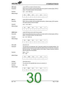
The following table shows the C1, C2 and R1 value according different crystal values.
Crystal or Resonator
4MHz Crystal
C1, C2
0pF
R1
10kW
12kW
12kW
10kW
10kW
10kW
27kW
9.1kW
10kW
10kW
4MHz Resonator (3 pin)
4MHz Resonator (2 pin)
3.58MHz Crystal
0pF
10pF
0pF
3.58MHz Resonator (2 pin)
2MHz Crystal & Resonator (2 pin)
1MHz Crystal
25pF
25pF
35pF
300pF
300pF
300pF
480kHz Resonator
455kHz Resonator
429kHz Resonator
Note: The resistance and capacitance for reset circuit should be designed in such a way as to ensure that the VDD is
stable and remains within a valid operating voltage range before bringing RES to high.
²*² Make the length of the wiring, which is connected to the RES pin as short as possible, to avoid noise
interference.
Rev. 1.90
26
May 17, 2004

 HOLTEK [ HOLTEK SEMICONDUCTOR INC ]