HT36A1
H
A
L
T
TMR0C Bit 4 to enable/disable timer counting
W
a
r
m
R
e
s
e
t
W
T
D
T
e
(1=enable; 0=disable)
W
D
T
i
m
-
o
u
t
TMR0C Bit 3, always write ²0².
TMR0C Bit 5, always write ²0².
TMR0C Bit 6, always write ²0².
TMR0C Bit 7, always write ²1².
R
e
s
e
t
R
E
S
C
o
l
d
S
S
T
R
e
s
e
t
1
0
-
s
t
a
g
e
O
S
C
I
R
i
p
p
l
e
C
o
u
n
t
e
r
D
a
t
a
B
u
s
T
i
m
e
r
0
/
1
P
o
w
e
r
-
o
n
D
e
t
e
c
t
i
n
g
R
e
l
o
a
d
P
r
e
l
o
a
d
R
e
g
i
s
t
e
r
S
y
s
t
e
m
8
-
s
t
a
g
e
P
r
e
s
c
a
l
e
r
C
l
o
c
k
/
8
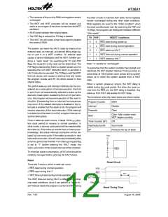
Reset Configuration
T
0
F
T
i
m
e
r
0
/
1
O
v
e
r
f
l
o
w
T
O
N
Timer 0/1
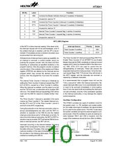
Timer 0 is an 8-bit counter, and its clock source comes
from the system clock divided by an 8-stage prescaler.
There are two registers related to Timer 0; TMR0L(0DH)
and TMR0C(0EH). One physical registers are mapped
to TMR0L location; writing TMR0L makes the starting
value be placed in the Timer 0 preload register and
reading the TMR0 gets the contents of the Timer 0 coun-
ter. The TMR0C is a control register, which defines the
division ration of the prescaler and counting enable or
disable.
Timer 0/1
Input/Output Ports
There are 24 bidirectional input/output lines labeled
from PA to PC, which are mapped to the data memory of
[12H], [14H], [16H] respectively. All these I/O ports can
be used for input and output operations. For input oper-
ation, these ports are non-latching, that is, the inputs
must be ready at the T2 rising edge of instruction MOV
A,[m] (m=12H, 14H or 16H). For output operation, all
data is latched and remains unchanged until the output
latch is rewritten.
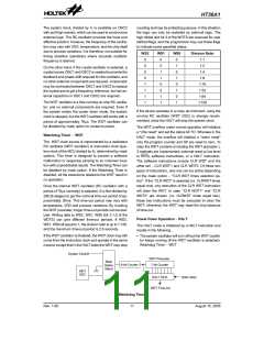
Writing data to B2, B1 and B0 (bits 2, 1, 0 of TMR0C)
can yield various clock sources.
One the Timer 0 starts counting, it will count from the
current contents in the counter to FFH. Once an over-
flow occurs, the counter is reloaded from a preload reg-
ister, and generates an interrupt request flag (T0F; bit 2
of INTCH). To enable the counting operation, the timer
On bit (TON; bit 4 of TMR0C) should be set to ²1². For
proper operation, bit 7 of TMR0C should be set to ²1²
and bit 3, bit 6 should be set to ²0².
Each I/O line has its own control register (PAC, PBC,
PCC) to control the input/output configuration. With this
control register, CMOS output or Schmitt trigger input
with or without pull-high resistor (mask option) struc-
tures can be reconfigured dynamically under software
control. To function as an input, the corresponding latch
of the control register must write a ²1². The pull-high re-
sistance will exhibit automatically if the pull-high option
is selected. The input source also depends on the con-
trol register. If the control register bit is ²1², input will
read the pad state. If the control register bit is ²0², the
contents of the latches will move to the internal bus. The
latter is possible in ²read-modify-write² instruction. For
output function, CMOS is the only configuration. These
control registers are mapped to locations 13H, 15H and
17H.
There are two registers related to the Timer Counter1;
TMR1L(10H), TMR1C(11H). The Timer Counter 1 oper-
ates in the same manner as Timer Counter 0.
TMR0C/TMR1C
T0F
B2
0
B1
B0
0
0
SYS CLK/16
SYS CLK/32
SYS CLK/64
SYS CLK/128
SYS CLK/256
SYS CLK/512
SYS CLK/1024
SYS CLK/2048
0
0
1
After a chip reset, these input/output lines remain at high
levels or floating (mask option). Each bit of these in-
put/output latches can be set or cleared by the SET [m].i
or CLR [m].i (m=12H, 14H or 16H) instruction.
0
1
0
0
1
1
1
0
0
1
0
1
Some instructions first input data and then follow the
output operations. For example, the SET [m].i, CLR
[m].i, CPL [m] and CPLA [m] instructions read the entire
port states into the CPU, execute the defined operations
(bit-operation), and then write the results back to the
latches or the accumulator.
1
1
0
1
1
1
Each line of port A has the capability to wake-up the de-
vice.
Rev. 1.00
14
August 15, 2005

 HOLTEK [ HOLTEK SEMICONDUCTOR INC ]