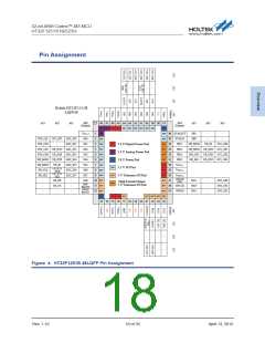
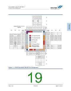
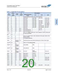
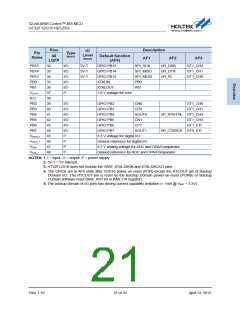
ꢃꢅ-bit �RM Coꢁtex™-Mꢃ MCU
HTꢃꢅF1ꢅ51/51B/5ꢅ/5ꢃ
Electrical Characteristics
4
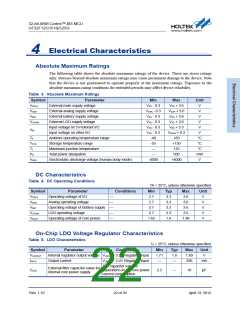
Absolute Maximum Ratings
The following table shows the absolute maximum ratings of the device. These are stress ratings
only. Stresses beyond absolute maximum ratings may cause permanent damage to the device. Note
that the device is not guaranteed to operate properly at the maximum ratings. Exposure to the
absolute maximum rating conditions for extended periods may affect device reliability.
Table 3. Absolute Maximum Ratings
Symbol
VDDꢃꢃ
Parameter
Min
VSS - 0.ꢃ
VSS� - 0.ꢃ
VSS - 0.ꢃ
VSS - 0.ꢃ
VSS - 0.ꢃ
VSS - 0.ꢃ
-40
Max
VSS + ꢃ.6
VSS� + ꢃ.6
VSS + ꢃ.6
VSS + ꢃ.6
VSS + 5.5
VDDꢃꢃ + 0.ꢃ
+85
Unit
V
Exteꢁnaꢂ main suꢀꢀꢂy voꢂtage
VDD�
Exteꢁnaꢂ anaꢂog suꢀꢀꢂy voꢂtage
Exteꢁnaꢂ batteꢁy suꢀꢀꢂy voꢂtage
Exteꢁnaꢂ LDO suꢀꢀꢂy voꢂtage
V
VB�T
V
VLDOIN
V
Inꢀut voꢂtage on 5V-toꢂeꢁant I/O
Inꢀut voꢂtage on otheꢁ I/O
V
VIN
V
T�
�mbient oꢀeꢁating temꢀeꢁatuꢁe ꢁange
Stoꢁage temꢀeꢁatuꢁe ꢁange
°C
°C
°C
mW
V
TSTG
TJ
-55
+150
Maximum junction temꢀeꢁatuꢁe
Totaꢂ ꢀoweꢁ dissiꢀation
—
1ꢅ5
PD
—
500
VESD
Eꢂectꢁostatic dischaꢁge voꢂtage (human body mode)
-4000
+4000
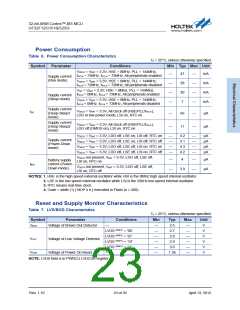
DC Characteristics
Table 4. DC Operating Conditions
TA = 25°C, unless otherwise specified.
Symbol
VDDꢃꢃ
Parameter
Conditions
Min
ꢅ.7
Typ
ꢃ.ꢃ
ꢃ.ꢃ
ꢃ.ꢃ
ꢃ.ꢃ
1.8
Max
ꢃ.6
Unit
V
Oꢀeꢁating voꢂtage of I/O
—
—
—
—
—
VDD�
�naꢂog oꢀeꢁating voꢂtage
Oꢀeꢁating voꢂtage of Batteꢁy suꢀꢀꢂy
LDO oꢀeꢁating voꢂtage
ꢅ.7
ꢃ.6
V
VB�T
ꢅ.7
ꢃ.6
V
VLDOIN
VDD18
ꢅ.7
ꢃ.6
V
Oꢀeꢁating voꢂtage of coꢁe ꢀoweꢁ
1.6ꢅ
1.98
V
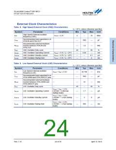
On-Chip LDO Voltage Regulator Characteristics
Table 5. LDO Characteristics
T� = ꢅ5°C, unless otherwise specified.
Symbol
VLDOOUT
IDD18
Parameter
Conditions
Min
1.71
—
Typ
1.8
—
Max
1.89
ꢅ00
Unit
V
Inteꢁnaꢂ ꢁeguꢂatoꢁ outꢀut voꢂtage VLDOIN = ꢃ.ꢃV Reguꢂatoꢁ inꢀut
Outꢀut cuꢁꢁent
VLDOIN = ꢅ.4V Reguꢂatoꢁ inꢀut
m�
The caꢀacitoꢁ vaꢂue is
deꢀendent on the coꢁe ꢀoweꢁ
cuꢁꢁent consumꢀtion
External filter capacitor value for
inteꢁnaꢂ coꢁe ꢀoweꢁ suꢀꢀꢂy
CLDO
ꢅ.ꢅ
—
10
μF
Rev. 1.10
ꢅꢅ of ꢃ5
�ꢀꢁiꢂ 1ꢃꢄ ꢅ01ꢅ

 HOLTEK [ HOLTEK SEMICONDUCTOR INC ]