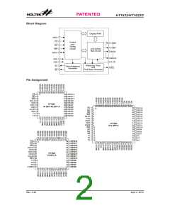
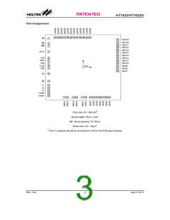
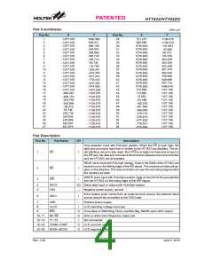
PATENTED
HT1622/HT1622G
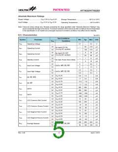
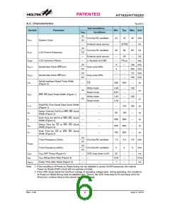
A.C. Characteristics
Ta=25°C
Test Conditions
Symbol
Parameter
Min.
Typ. Max. Unit
VDD
3V
5V
¾
Conditions
On-chip RC oscillator
External clock source
On-chip RC oscillator
24
¾
48
32
32768
64
40
¾
80
kHz
Hz
fSYS
System Clock
3V
5V
¾
Hz
fLCD
LCD Frame Frequency
External clock source
n: Number of COM
64
Hz
¾
¾
4
¾
¾
tCOM
n/fLCD
LCD Common Period
sec
¾
3V
5V
3V
5V
150 kHz
300 kHz
¾
¾
¾
¾
fCLK1
Serial Data Clock (WR pin)
Duty cycle 50%
4
75
kHz
¾
¾
fCLK2
Serial Data Clock (RD pin)
Duty cycle 50%
CS
150 kHz
Serial Interface Reset Pulse Width
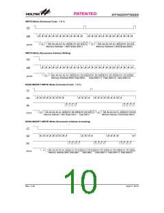
(Figure 3)
tCS
500
600
ns
¾
¾
Write mode
Read mode
Write mode
Read mode
3.34
6.67
1.67
3.34
125
¾
¾
¾
¾
¾
3V
ms
tCLK
WR, RD Input Pulse Width (Figure 1)
125
¾
5V
ms
Rise/Fall Time Serial Data Clock Width
(Figure 1)
tr, tf
120
120
600
600
800
160
¾
ns
ns
ns
ns
ns
¾
¾
¾
¾
¾
¾
¾
¾
¾
¾
¾
Setup Time for DATA to WR, RD Clock
Width (Figure 2)
tsu
60
Hold Time for DATA to WR, RD, Clock
Width (Figure 2)
th
500
500
700
¾
Setup Time for CS to WR, RD Clock
Width (Figure 3)
tsu1
¾
Hold Time for CS to WR, RD Clock
Width (Figure 3)
th1
¾
3V
5V
3V
5V
¾
Tone Frequency (2kHz)
Tone Frequency (4kHz)
On-chip RC oscillator
On-chip RC oscillator
1.5
3
2.0
4
2.5
5
kHz
kHz
fTONE
tOFF
tSR
VDD OFF Times (Figure 4)
VDD drop down to 0V
20
0.05
1
ms
V/ms
ms
¾
¾
¾
¾
¾
¾
VDD Rising Slew Rate (Figure 4)
Delay Time after Reset (Figure 4)
¾
¾
tRSTD
¾
¾
Note: 1. If the conditions of Power-on Reset timing are not satisfied in power On/Off sequence, the internal
Power-on Reset (POR) circuit will not operate normally.
2. If the VDD drops below the minimum voltage of operating voltage spec. during operating, the conditions
of Power-on Reset timing must be satisfied also. That is, the VDD must drop to 0V and keep at 0V for
20ms (min.) before rising to the normal operating voltage.
Rev. 2.40
6
April 2, 2012
图片预览")
 HOLTEK [ HOLTEK SEMICONDUCTOR INC ]