PATENTED
HT1622/HT1622G
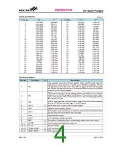
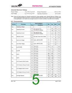
Pad Coordinates
Unit: mm
Pad No.
X
Y
Pad No.
X
Y
1
1090.589
905.211
28
29
30
31
32
33
34
35
36
37
38
39
40
41
42
43
44
45
46
47
48
49
50
51
52
53
54
721.077
820.095
-1077.075
-1077.075
-1077.075
-1077.075
-1077.037
-1077.075
-1077.037
-1077.075
-1077.075
-1077.075
-1077.075
-1077.075
-1077.075
-1077.075
-1077.075
-1077.075
-589.281
-490.179
-304.799
-205.699
-20.319
-1129.575
-1129.575
-141.904
-42.885
56.215
2
3
806.109
1076.900
1076.900
1076.900
1076.900
1076.900
1076.900
1076.900
1076.900
1076.900
1076.900
1076.900
1076.900
1076.900
213.669
4
594.542
5
359.680
6
260.745
155.234
254.335
353.354
452.456
551.474
650.576
749.594
848.695
947.714
1046.816
1127.150
1127.150
1127.150
1127.150
1127.150
1127.150
1127.150
1127.150
1127.150
1127.150
1127.150
1127.150
7
162.710
8
63.734
9
-34.789
10
11
12
13
14
15
16
17
18
19
20
21
22
23
24
25
26
27
-238.247
-519.705
-677.315
-776.416
-875.435
-974.536
-1073.554
-1129.575
-1129.575
-1129.575
-1129.575
-1129.575
-1129.575
-1129.575
-1129.575
-1129.575
-1129.575
-1129.575
114.650
15.550
-83.469
-182.570
-281.590
-380.690
-479.710
-578.810
-677.829
-776.931
-875.949
78.736
225.736
324.836
423.856
522.957
621.975
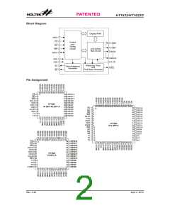
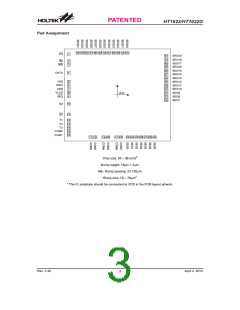
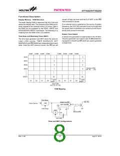
Pad Description
Pad No.
Pad Name
I/O
Description
Chip selection input with Pull-high resistor. When the CS is logic high, the
data and command read from or written to the HT1622 are disabled. The se-
rial interface circuit is also reset. But if CS is at logic low level and is input to
the CS pad, the data and command transmission between the host controller
and the HT1622 are all enabled.
1
CS
I
READ clock input with Pull-high resistor. Data in the RAM of the HT1622 are
clocked out on the falling edge of the RD signal. The clocked out data will ap-
pear on the data line. The host controller can use the next rising edge to latch
the clocked out data.
2
3
RD
I
I
WRITE clock input with Pull-high resistor. Data on the DATA line are latched
into the HT1622 on the rising edge of the WR signal.
WR
4
5
DATA
VSS
I/O Serial data input or output with Pull-high resistor
Negative power supply, ground
¾
If the system clock comes from an external clock source, the external clock
source should be connected to the OSCI pad.
6
OSCI
I
7
VDD
Positive power supply
¾
I
8
VLCD
IRQ
LCD operating voltage input pad
Time base or Watchdog Timer overflow flag, NMOS open drain output
2kHz or 4kHz tone frequency output pair
Not connected
9
O
O
I
10, 11
12~14
15~22
23~54
BZ, BZ
T1~T3
COM0~COM7
SEG0~SEG31
O
O
LCD common outputs
LCD segment outputs
Rev. 2.40
4
April 2, 2012
图片预览")
 HOLTEK [ HOLTEK SEMICONDUCTOR INC ]