ICL7135
7.
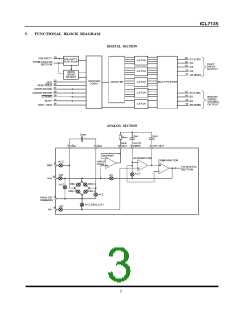
PRINCIPLES OF OPERATION
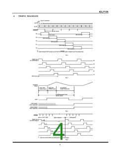
A measurement cycle for the ICL7135 consists of the following four phases.
1. Auto-Zero Phase.
The internal IN+ and IN- inputs are disconnected from the terminals and internally connected to ANALOG COMMON.
The reference capacitor is charged to the reference voltage. The system is configured in a closed loop and the auto-zero
capacitor is charged to compensate for offset voltages in the buffer amplifier, integrator, and comparator. The auto-zero
accuracy is limited only by the system noise, and the overall offset, as referred to the input, is less than 10 µV.
2. Signal Integrate Phase.
The auto-zero loop is opened and the internal IN+ and IN- inputs are connected to the external terminals.
The differential voltage between these inputs is integrated for a fixed period of time. When the input signal has no
return with respect to the converter power supply, IN- can be tied to ANALOG COMMON to establish the correct
common-mode voltage. Upon completion of this phase, the polarity of the input signal is recorded.
3. Deintegrate Phase.
The reference is used to perform the deintegrate task. The internal IN- is internally connected to ANALOG COMMON
and IN+ is connected across the previously charged reference capacitor. The recorded polarity of the input signal
ensures that the capacitor is connected with the correct polarity so that the integrator output polarity returns to zero. The
time required for the output to return to zero is proportional to the amplitude of the input signal. The return time is
displayed as a digital reading and is determined by the equation 10000 x (VID/VREF). The maximum or full-scale
conversion occurs when VID is two times VREF
.
4. Zero Integrator Phase.
The internal IN- is connected to ANALOG COMMON. The system is configured in a closed loop to cause the
integrator output to return to zero. Typically, this phase requires 100 to 200 clock pulses. However, after an over-range
conversion, 6200 pulses are required.
8.
DESCRIPTION OF ANALOG CIRCUITS
• Input Signal Range
The common mode range of the input amplifier extends from 1V above the negative supply to 1V below the positive
supply. Within this range, the common-mode rejection ratio (CMRR) is typically 86 dB. Both differential and common-
mode voltages cause the integrator output to swing. Therefore, care must be exercised to ensure that the integrator
output does not become saturated.
• Analog Common
Analog common (ANALOG COMMON) is connected to the internal IN- during the auto-zero, deintegrate, and zero
integrator phases. When IN- is connected to a voltage that is different from analog common during the signal integrate
phase, the resulting common-mode voltage is rejected by the amplifier. However, in most applications, IN- is set at a
known fixed voltage (i.e., power supply common for instance). In this application, analog common should be tied to the
same point, thus removing the common-mode voltage from the converter. Removing the common-mode voltage in this
manner slightly increases conversion accuracy.
• Reference
The reference voltage is positive with respect to analog common. The accuracy of the conversion result is dependent
upon the quality of the reference.
5

 HN [ NANJING HONANO ELECTRONIC CO., LTD. ]