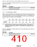
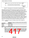
Table 19.6 Erase Blocks and Corresponding Bits
Register
Bit
0
Block
LB0
Address
Size
EBR1
H'1000 to H'1FFF
H'2000 to H'3FFF
H'5FFF
4 kbytes
8 kbytes
8
1
LB1
2LB2H'4000
LB3
H'0000
SB1
2SB2H'0100
to
to
kbytes
3
H'6000 to H'7FFF
to
8 kbytes
8
EBR20
SB0
H'007F
12 bytes
1
H'0080 to H'00FF
H'017F
128 bytes
12 bytes
128 bytes
512 bytes
1 kbyte
1 kbyte
1 kbyte
8
3
4
5
6
7
SB3
SB4
H'0180 to H'01FF
H'0200 to H'03FF
H'0400 to H'07FF
H'0800 to H'0BFF
H'0C00 to H'0FFF
SB5
SB6
SB7
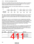
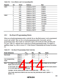
19.3
On-Board Programming Modes
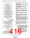
When an on-board programming mode is selected, the on-chip flash memory can be programmed,
erased, and verified. There are two on-board programming modes: boot mode, and user
programming mode. These modes are selected by inputs at the mode pins (MD1 and MD0) and
FVPP pin. Table 19.7 indicates how to select the on-board programming modes. For details on
applying voltage VPP, refer to section 19.7, Flash Memory Programming and Erasing Precautions
(5).
Table 19.7 On-Board Programming Mode Selection
Mode Selections
FVPP
MD1
*212 V 12 V*
12 V*
MD0
0
Notes
0: VIL
1: VIH
Boot
mode
Mode
Mode 3
1
User
mode
programming
Mode 3
Mode
21
0
1
1
Note: * For details on the timing of 12 V application, see notes 6 to 8 in the Notes on Use of Boot
Mode at the end of this section.
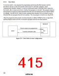
In boot mode, the mode control register (MDCR) can be used to monitor the mode (mode 2
or 3) in the same way as in normal mode.
Example: Set the mode pins for mode 2 boot mode (MD1 = 12 V, MD0 = 0 V).
If the mode select bits of MDCR are now read, they will indicate mode 2 (MDS1 = 1,
MDS0 = 0).
385

 HITACHI [ HITACHI SEMICONDUCTOR ]