PDF
最近搜索
热门搜索
发布采购

| 型号: | HD6473434F16 |
| PDF下载: | 下载PDF文件 查看货源 |
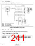
| 内容描述: | 12伏不能应用于S -掩模模型(单电源规格) ,因为这可能会永久损坏设备。 [12 V must not be applied to the S-mask model (single-power-supply specification), as this may permanently damage the device.] |
| 分类和应用: | 外围集成电路微控制器可编程只读存储器时钟 |
| 文件页数/大小: | 752 页 / 2557 K |
| 品牌: |  HITACHI [ HITACHI SEMICONDUCTOR ] HITACHI [ HITACHI SEMICONDUCTOR ] |
专业IC领域供求交易平台:提供全面的IC Datasheet资料和资讯,Datasheet 1000万数据,IC品牌1000多家。