Similarly, when the BUFEB bit in TCR is set to 1, ICRD is used as a buffer register for ICRB.
When input capture is buffered, if the two input edge bits are set to different values (IEDGA ≠
IEDGC or IEDGB ≠ IEDGD), then input capture is triggered on both the rising and falling edges
of the FTIA or FTIB input signal. If the two input edge bits are set to the same value (IEDGA =
IEDGC or IEDGB = IEDGD), then input capture is triggered on only one edge. See table 8.3.
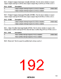
Table 8.3 Buffered Input Capture Edge Selection (Example)
IEDGA
IEDGC
Input Capture Edge
0
0
1
0
1
Captured on falling edge of input capture A (FTIA)
(Initial value)
Captured on both rising and falling edges of input capture A (FTIA)
Captured on rising edge of input capture A (FTIA)
1
Because the input capture registers are 16-bit registers, a temporary register (TEMP) is used when
they are read. See section 8.3, CPU Interface, for details.
To ensure input capture, the width of the input capture pulse should be at least 1.5 system clock
periods (1.5·ø). When triggering is enabled on both edges, the input capture pulse width should be
at least 2.5 system clock periods.
The input capture registers are initialized to H'0000 by a reset and in the standby modes.
161

 HITACHI [ HITACHI SEMICONDUCTOR ]