8.2
Register Descriptions
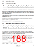
8.2.1
Free-Running Counter (FRC)
Bit
15 14 13 12 11 10
9
0
8
0
7
0
6
0
5
0
4
0
3
0
2
0
1
0
0
0
Initial value
0
0
0
0
0
0
Read/Write R/W R/W R/W R/W R/W R/W R/W R/W R/W R/W R/W R/W R/W R/W R/W R/W
FRC is a 16-bit readable/writable up-counter that increments on an internal pulse generated from a
clock source. The clock source is selected by the clock select 1 and 0 bits (CKS1 and CKS0) of the
timer control register (TCR).
When FRC overflows from H'FFFF to H'0000, the overflow flag (OVF) in the timer control/status
register (TCSR) is set to 1.
Because FRC is a 16-bit register, a temporary register (TEMP) is used when FRC is written or
read. See section 8.3, CPU Interface, for details.
FRC is initialized to H'0000 by a reset and in the standby modes.
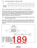
8.2.2
Output Compare Registers A and B (OCRA and OCRB)
Bit
15 14 13 12 11 10
9
8
7
6
5
4
1
3
1
2
1
1
1
0
1
Initial value
1
1
1
1
1
1
1
1
1
1
1
Read/Write R/W R/W R/W R/W R/W R/W R/W R/W R/W R/W R/W R/W R/W R/W R/W R/W
OCRA and OCRB are 16-bit readable/writable registers, the contents of which are continually
compared with the value in the FRC. When a match is detected, the corresponding output compare
flag (OCFA or OCFB) is set in the timer control/status register (TCSR).
In addition, if the output enable bit (OEA or OEB) in the timer output compare control register
(TOCR) is set to 1, when the output compare register and FRC values match, the logic level
selected by the output level bit (OLVLA or OLVLB) in TOCR is output at the output compare pin
(FTOA or FTOB). Following a reset, the FTOA and FTOB output levels are 0 until the first
compare-match.
OCRA and OCRB share the same address. They are differentiated by the OCRS bit in TOCR. A
temporary register (TEMP) is used for write access, as explained in section 8.3, CPU Interface.
OCRA and OCRB are initialized to H'FFFF by a reset and in the standby modes.
159

 HITACHI [ HITACHI SEMICONDUCTOR ]