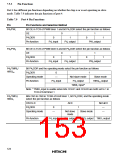
Pin
Pin Functions and Selection Method
P43/TMCI1/
HIRQ11
Bit P43DDR and the operating mode select the pin function as follows
P43DDR
0
—
1
Operating mode
Pin function
Not slave mode
P43 output
Slave mode
P43 input
HIRQ11 output
TMCI1 input*
Note: * TMCI1 input is usable when bits CKS2 to CKS0 in TCR of 8-bit timer 1
select an external clock source
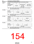
P42/TMRI0
P41/TMO0
P40/TMCI0
P42DDR
0
1
Pin function
P42 input
P42 output
TMRI0 input*
Note: * TMRI0 input is usable when bits CCLR1 and CCLR0 are both set to 1 in
TCR of 8-bit timer 0
Bits OS3 to OS0 in TCSR of 8-bit timer 0 and bit P41DDR select the pin function
as follows
OS3 to 0
P41DDR
All 0
Not all 0
0
1
0
1
Pin function
P41 input
P41 output
TMO0 output
P40DDR
0
P40 input
1
Pin function
P40 output
TMCI0 input*
Note: * TMCI0 input is usable when bits CKS2 to CKS0 in TCR of 8-bit timer 0
select an external clock source
125

 HITACHI [ HITACHI SEMICONDUCTOR ]