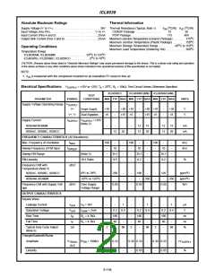
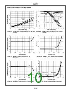
ICL8038
Reducing Distortion
output can be made TTL compatible (load resistor con-
nected to +5V) while the waveform generator itself is pow-
ered from a much higher voltage.
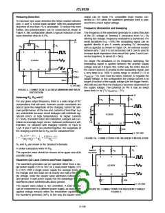
To minimize sine wave distortion the 82kΩ resistor between
pins 11 and 12 is best made variable. With this arrangement
distortion of less than 1% is achievable. To reduce this even
further, two potentiometers can be connected as shown in
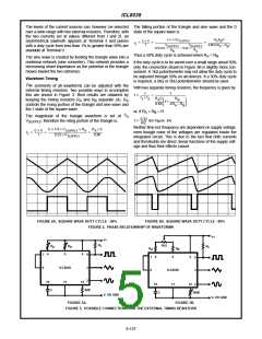
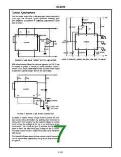
Frequency Modulation and Sweeping
Figure 4; this configuration allows a typical reduction of sine The frequency of the waveform generator is a direct function
wave distortion close to 0.5%.
of the DC voltage at Terminal 8 (measured from V+). By
altering this voltage, frequency modulation is performed. For
small deviations (e.g. ±10%) the modulating signal can be
applied directly to pin 8, merely providing DC decoupling
with a capacitor as shown in Figure 5A. An external resistor
between pins 7 and 8 is not necessary, but it can be used to
increase input impedance from about 8kΩ (pins 7 and 8 con-
nected together), to about (R + 8kΩ).
V+
1kΩ
R
L
R
R
B
A
4
5
6
1
7
9
3
8
ICL8038
For larger FM deviations or for frequency sweeping, the
modulating signal is applied between the positive supply
voltage and pin 8 (Figure 5B). In this way the entire bias for
the current sources is created by the modulating signal, and
a very large (e.g. 1000:1) sweep range is created (f = 0 at
2
10
11
12
100kΩ
10kΩ
10kΩ
C
V
= 0). Care must be taken, however, to regulate the
SWEEP
100kΩ
supply voltage; in this configuration the charge current is no
longer a function of the supply voltage (yet the trigger thresh-
olds still are) and thus the frequency becomes dependent on
V- OR GND
the supply voltage. The potential on Pin 8 may be swept
1
FIGURE 4. CONNECTION TO ACHIEVE MINIMUM SINE WAVE
DISTORTION
down from V+ by ( / V
- 2V).
SUPPLY
3
V+
Selecting R , R and C
A
B
R
L
R
R
A
B
For any given output frequency, there is a wide range of RC
combinations that will work, however certain constraints are
placed upon the magnitude of the charging current for opti-
mum performance. At the low end, currents of less than 1µA
are undesirable because circuit leakages will contribute sig-
nificant errors at high temperatures. At higher currents
(I > 5mA), transistor betas and saturation voltages will con-
tribute increasingly larger errors. Optimum performance will,
therefore, be obtained with charging currents of 10µA to
1mA. If pins 7 and 8 are shorted together, the magnitude of
4
5
6
7
8
9
3
R
ICL8038
11
FM
2
10
12
C
81K
the charging current due to R can be calculated from:
A
V- OR GND
R
× (V+ – V-)
1
1
0.22(V+ – V-)
---------------------------------------- -------
I =
×
= -----------------------------------
FIGURE 5A. CONNECTIONS FOR FREQUENCY MODULATION
V+
(R + R )
R
R
1
2
A
A
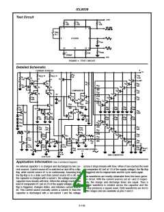
R and R are shown in the Detailed Schematic.
1
2
A similar calculation holds for R .
B
R
L
SWEEP
VOLTAGE
R
R
A
B
The capacitor value should be chosen at the upper end of its
possible range.
4
5
6
9
3
Waveform Out Level Control and Power Supplies
The waveform generator can be operated either from a sin-
gle power supply (10V to 30V) or a dual power supply (±5V
to ±15V). With a single power supply the average levels of
the triangle and sine wave are at exactly one-half of the sup-
ply voltage, while the square wave alternates between V+
and ground. A split power supply has the advantage that all
waveforms move symmetrically about ground.
8
ICL8038
11
2
10
12
C
81K
V- OR GND
The square wave output is not committed. A load resistor
can be connected to a different power supply, as long as the
applied voltage remains within the breakdown capability of
the waveform generator (30V). In this way, the square wave
FIGURE 5B. CONNECTIONS FOR FREQUENCY SWEEP
FIGURE 5.
8-158

 HARRIS [ HARRIS CORPORATION ]