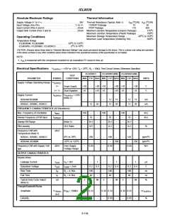
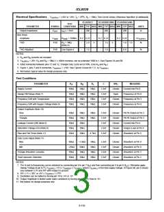
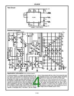
ICL8038
The levels of the current sources can, however, be selected The falling portion of the triangle and sine wave and the 0
over a wide range with two external resistors. Therefore, with state of the square wave is:
the two currents set at values different from I and 2I, an
R
R C
C × 1/3V
C × V
SUPPLY
A B
asymmetrical sawtooth appears at Terminal 3 and pulses
with a duty cycle from less than 1% to greater than 99% are
available at Terminal 9.
t
= ------------ = ----------------------------------------------------------------------------------- = -------------------------------------
2
1 V V
0.66(2R – R
)
SUPPLY
SUPPLY
A
B
------------------------
------------------------
2(0.22)
– 0.22
R
R
B
A
Thus a 50% duty cycle is achieved when R = R .
A
B
The sine wave is created by feeding the triangle wave into a
nonlinear network (sine converter). This network provides a
decreasing shunt impedance as the potential of the triangle
moves toward the two extremes.
If the duty cycle is to be varied over a small range about 50%
only, the connection shown in Figure 3B is slightly more con-
venient. A 1kΩ potentiometer may not allow the duty cycle to
be adjusted through 50% on all devices. If a 50% duty cycle
is required, a 2kΩ or 5kΩ potentiometer should be used.
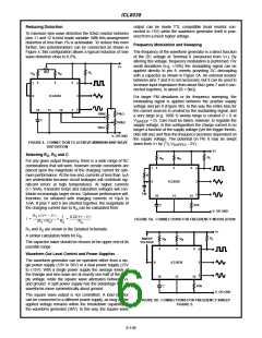
Waveform Timing
The symmetry of all waveforms can be adjusted with the
external timing resistors. Two possible ways to accomplish
this are shown in Figure 3. Best results are obtained by
With two separate timing resistors, the frequency is given by:
1
+ t
1
f = --------------- = -----------------------------------------------------
t
R C
A
R
1
2
keeping the timing resistors R and R separate (A). R
B
A
B
A
------------
1 + -------------------------
0.66
2R – R
controls the rising portion of the triangle and sine wave and
A
B
the 1 state of the square wave.
or, if R = R = R
A
B
1
The magnitude of the triangle waveform is set at
/
3
0.33
-----------
RC
V
; therefore the rising portion of the triangle is,
f =
(for Figure 3A)
SUPPLY
Neither time nor frequency are dependent on supply voltage,
even though none of the voltages are regulated inside the
integrated circuit. This is due to the fact that both currents
and thresholds are direct, linear functions of the supply volt-
age and thus their effects cancel.
C × 1/3 × V
× R
R × C
A
0.66
C × V
I
SUPPLY
A
t
= -------------- = ----------------------------------------------------------------- = ------------------
1
0.22 × V
SUPPLY
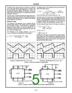
FIGURE 2A. SQUARE WAVE DUTY CYCLE - 50%
FIGURE 2B. SQUARE WAVE DUTY CYCLE - 80%
FIGURE 2. PHASE RELATIONSHIP OF WAVEFORMS
V+
V+
R
L
1kΩ
R
R
R
A
B
L
R
R
B
A
4
5
6
7
8
9
3
4
5
6
7
9
3
ICL8038
11
8
ICL8038
11
2
10
12
10
12
2
C
82K
C
100K
V- OR GND
V- OR GND
FIGURE 3A.
FIGURE 3B.
FIGURE 3. POSSIBLE CONNECTIONS FOR THE EXTERNAL TIMING RESISTORS
8-157

 HARRIS [ HARRIS CORPORATION ]