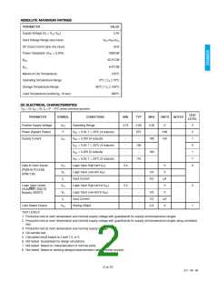
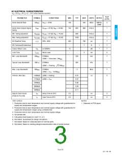
DETAILED DESCRIPTION
The GS9032 Serializer is a bipolar integrated circuit used to
convert parallel data into a serial format according to the
SMPTE 259M standard. The device encodes both eight and
ten bit TTL-compatible parallel signals producing serial
data rates up to 540Mb/s. It operates from a single five volt
supply and is packaged in a 44 pin TQFP.
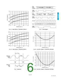
about the centre frequency. The single external resistor,
VCO, sets the VCO frequency (see Figure 12).
R
4. VCO CENTRE FREQUENCY SELECTION
For a given RVCO value, the VCO can oscillate at one of two
frequencies. When SS0=logic 1, the VCO centre frequency
corresponds to the ƒL curve. For SS0=logic 0, the VCO
centre frequency corresponds to the ƒH curve (ƒH is
approximately 1.5 x ƒL).
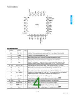
Functional blocks within the device include the input
latches, sync detector, parallel to serial converter, SMPTE
scrambler, NRZ to NRZI converter, internal cable driver, PLL
for 10x parallel clock multiplication and lock detect. The
parallel data (PD0-PD9) and parallel clock (PCLKIN) are
applied via pins 1 through 11 respectively.
800
700
600
500
400
1. SYNC DETECTOR
The sync detector makes the system compatible with eight
or ten bit data. It looks for the reserved words 000-003 and
3FC-3FF in ten bit hexadecimal, or 00 and FF in eight bit
hexadecimal, used in the TRS-ID sync word. When the
occurrence of either all zeros or all ones at inputs PD2-PD9
is detected, the lower two bits PD0 and PD1 are forced to
zeros or ones respectively. For non-SMPTE standard
parallel data, the sync detector can be disabled through a
logic input, Sync Detect Disable (44).
ƒ
H
300
SSO=0
200
ƒ
L
100
0
SSO=1
0
200 400 600
800
R
1000 1200 1400 1600 1800
(Ω)
VCO
Fig. 12
2. SCRAMBLER
The recommended RVCO value for auto rate SMPTE 259M
applications is 374Ω (see the Typical Application Circuit).
This value prevents false standards indication in auto mode.
For non-SMPTE applications (where data rates are x2
harmonically related) use Figure 12 to determine the RVCO
values.
The scrambler is a linear feedback shift register used to
pseudo-randomize the incoming serial data according to
the fixed polynomial (X9+X4+1). This minimizes the DC
component in the output serial data stream. The NRZ to
NRZI converter uses another polynomial (X+1) to convert a
long sequence of ones to a series of transitions, minimizing
polarity effects. These functions can be disabled by setting
the BYPASS pin (31) high.
The VCO and an internal divider generate the PLL clock.
Divider moduli of 1, 2, and 4 allow the PLL to lock to data
rates from 143Mb/s to 540Mb/s. The divider modulus is set
by the AUTO/MAN, and SS[2:0] pins (see Truth Table for
further details). In addition, a manually selectable modulus
8 divider allows operation at data rates as low as 18Mb/s
when RVCO is increased to 1kΩ.
3. PHASE LOCKED LOOP
The PLL performs parallel clock multiplication and provides
the timing signal for the serializer. It is composed of a
phase/frequency detector (with no dead zone), charge
pump, VCO, a divide-by-ten counter, and a divide-by-two
counter.
When the loop is not locked, the lock detect circuit mutes
the serial data outputs. When the loop is locked, the Lock
Detect output is available from pin 20 and is HIGH.
The phase/frequency detector allows a wider capture range
and faster lock time than with a phase discriminator alone.
The discrimination of frequency eliminates harmonic
locking. With this type of discriminator, the PLL can be over-
damped for good stability without sacrificing lock time.
The true and complement serial data, SDO and SDO, are
available from pins 24, 25, 27 and 28. These outputs drive
four 75Ω co-axial cables with SMPTE level serial digital
video signals. To disable the outputs from pins 27 and 28
(SDO1, SDO1), remove the resistor connected to the RSET1
pin (30) and float the SDO1 ENABLE pin (19).
The charge pump delivers a 'charge packet' to the loop
filter which is proportional to the system phase error.
Internal voltage clamps are used to constrain the loop filter
voltage between approximately 1.8 and 3.4 volts.
NOTE: Do NOT connect pin 19 to VCC
.
RSET calculation:
1.154 × RLOAD
RSET = --------------------------------------
VSDO
The VCO is a differential low phase noise, factory trimmed
design that provides increased immunity to PBC noise and
precise control of the VCO centre frequency. The VCO can
operate in excess of 800MHz and has a pull range of 15%
where RLOAD = RPULL-UP || Z
8 of 10
521 - 96 - 09

 GENNUM [ GENNUM CORPORATION ]