AC ELECTRICAL CHARACTERISTICS
VCC = 5V, VEE = 0V, TA = 0° – 70°C unless otherwise specified.
TEST
LEVEL
PARAMETER
SYMBOL
CONDITIONS
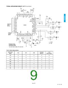
RVCO = 374Ω
MIN
TYP
MAX
UNITS
NOTES
Serial Data Bit Rate
BRSDO
143
-
540
Mb/s
SMPTE
259M
3
Serial Data Outputs Signal
Swing
VSDO
RLOAD = 37.5Ω, RSET = 54.9Ω
740
800
860
mVp-p
1
Min. Swing (adjusted)
Max. Swing (adjusted)
SD Rise/Fall Times
VSDOMIN
VSDOMAX
t , t
RLOAD = 37.5Ω, RSET = 73.2Ω
RLOAD = 37.5Ω, RSET = 43.2Ω
20% - 80%
-
-
600
1000
-
-
-
mVp-p
mVp-p
ps
7
1
7
400
700
r
f
SD Overshoot/Undershoot
Output Return Loss
Lock Time
-
15
-
-
7
-
%
dB
1
1
7
7
6
7
ORL
tLOCK
at 540MHz
Worst case
-
-
5
-
ms
kHz
Min. Loop Bandwidth
BWMIN
270Mb/s
-
220
LBWC = Grounded : BWMIN
Typical Loop Bandwidth
BWTYP
BWMAX
270Mb/s
-
-
500
1.7
-
-
kHz
7
LBWC = Floating :
BW
MIN
10
Max. Loop Bandwidth
270Mb/s
MHz
UI
7
3
LBWC = VCC : 10 BWMIN
Intrinsic Jitter (6σ)
143Mb/s LBWC = floating
177Mb/s LBWC = VCC
270Mb/s
-
0.07
0.07
0.08
0.09
0.11
-
-
-
-
-
-
360Mb/s
-
-
540Mb/s
-
-
Data & Clock Inputs
(PD[9:0] PCLKIN)
tSU
tH
Setup Time at 25°C
Hold Time at 25°C
2.5
2.0
-
-
ns
ns
3
3
-
TEST LEVELS
NOTES
1. Production test at room temperature and nominal supply voltage with guardbands for
supply and temperature ranges.
1. Depends on PCB layout.
2. Production test at room temperature and nominal supply voltage with guardbands for
supply and temperature ranges using correlated test.
3. Production test at room temperature and nominal supply voltage.
4. QA sample test.
5. Calculated result based on Level 1,2, or 3.
6. Not tested. Guaranteed by design simulations.
7. Not tested. Based on characterization of nominal parts.
8. Not tested. Based on existing design/characterization data of similar product.
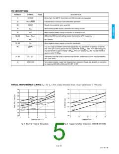
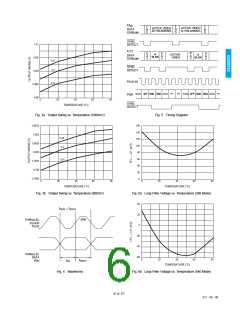
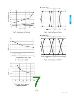
3 of 10
521 - 96 - 09

 GENNUM [ GENNUM CORPORATION ]