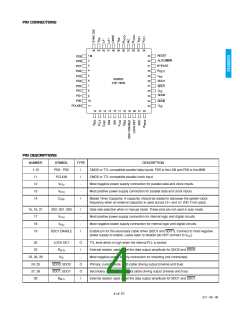
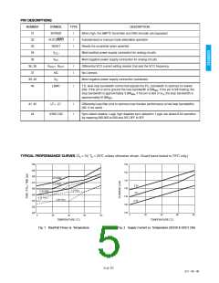
PIN CONNECTIONS
44 43 42 41 40 39 38 37 36 35 34
1
RESET
33
32
31
30
29
28
27
26
25
24
23
PD9
PD8
PD7
PD6
2
AUTO/MAN
BYPASS
3
4
R
SET1
5
V
PD5
PD4
EE
GS9032
6
SDO1
SDO1
TOP VIEW
7
PD3
PD2
V
8
EE
SDO0
SDO0
PD1
PD0
9
10
11
V
PCLKIN
EE
12 13 14 15 16 17 18 19 20 21 22
PIN DESCRIPTIONS
NUMBER
SYMBOL
TYPE
DESCRIPTION
1-10
11
PD9 - PD0
PCLKIN
VEE3
I
I
-
-
I
CMOS or TTL compatible parallel data inputs. PD0 is the LSB and PD9 is the MSB.
CMOS or TTL compatible parallel clock input.
12
Most negative power supply connection for parallel data and clock inputs.
Most positive power supply connection for parallel data and clock inputs.
13
VCC3
14
COSC
Master Timer Capacitor. A capacitor should be added to decrease the system clock
frequency when an external capacitor is used across LF+ and LF- (NC if not used).
15, 16, 21
SS2, SS1, SS0
VCC2
I
-
-
I
Data rate selection when in manual mode. These pins are not used in auto mode.
Most positive power supply connection for internal logic and digital circuits.
Most negative power supply connection for internal logic and digital circuits.
17
18
19
VEE2
SDO1 ENABLE
Enable pin for the secondary cable driver (SDO1 and SDO1). Connect to most negative
power supply to enable. Leave open to disable (do NOT connect to VCC).
20
22
LOCK DET
RSET0
O
I
TTL level which is high when the internal PLL is locked.
External resistor used to set the data output amplitude for SDO0 and SDO0.
Most negative power supply connection for shielding (not connected).
Primary, current mode, 75Ω cable driving output (inverse and true)
Secondary, current mode, 75Ω cable driving output (inverse and true)
External resistor used to set the data output amplitude for SDO1 and SDO1.
23, 26, 29
24, 25
27, 28
30
VEE
-
SDO0, SDO0
SDO1, SDO1
RSET1
O
O
I
4 of 10
521 - 96 - 09

 GENNUM [ GENNUM CORPORATION ]