APPLICATION INFORMATION
V
V
IN
OUT
The GM66150 series is high performance with low-
dropout voltage regulators, suitable for all moderate to
high-current voltage regulator applications. Their
350mV dropout voltage at full load makes them espe-
cially valuable in battery powered systems and as high
efficiency noise filters in "post-regulator" applications.
Unlike older NPN-pass transistor designs, for which
where the minimum dropout voltage is limited by the
base-emitter voltage drop and collector-emitter satura-
tion voltage, dropout performance of the PNP output of
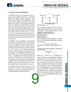
IN
OUT
GND
+
+
Figure 10. Linear regulators require only two
capacitors for operation.
Thermal Design
Linear regulators are simple to use. The most com-
plicated design parameters to consider are thermal
characteristics. Thermal design requires the follow-
ing application-specific parameters:
these devices is limited merely by the low V satura-
CE
Maximum ambient temperature, T
A
tion voltage. A trade-off for the low dropout voltage is a
varying base drive requirement. But, Gamma's PNP
process reduces this drive requirement to merely 1% of
the load current.
Output Current, I
OUT
Output Voltage, V
OUT
Input Voltage, V
IN
First, we calculate the power dissipation of the regu-
lator from these numbers and the device parameters
from this formula:
The GM66150 series of regulators is fully protected
from damage due to fault conditions. Current limiting is
provided. This limiting is linear, and output current un-
der overload conditions is constant. Thermal shutdown
disables the device when the die temperature exceeds
the 125°C maximum safe operating temperature.
Transient protection allows device (and load) survival
even when the input voltage spikes between -20V and
+60V. When the input voltage exceeds about 35V to
40V, the overvoltage sensor temporarily disables the
regulator. The output structure of these regulators al-
lows voltages in excess of the desired output voltage to
be applied without reverse current flow. GM66151 and
GM66152 versions offer a logic level ON/OFF control:
when disabled, the devices draw nearly zero current.
P = I
D
(1.01V - V
IN
)
OUT
OUT
where the ground current is approximated by 1% of
I
.
OUT
Then the heat sink thermal resistance is determined
with this formula:
T
- TA
J(MAX)
q
=
(q + q
JC
)
SA
CS
P
D
where T
125°C and q is between 0 and
CS
J(MAX)
2°C/W. The heat sink may be significantly reduced in
applications where the minimum input voltage is
known and is large compared with the dropout volt-
age. Use a series input resistor to drop excessive
voltage and distribute the heat between this resistor
and the regulator. The low dropout properties of
Gamma PNP regulators allow very significant reduc-
tions in regulator power dissipation and the associ-
ated heat sink without compromising performance.
When this technique is employed, a capacitor of at
least 0.1µF is needed directly between the input and
regulator ground.
An additional feature of this regulator family is a com-
mon pinout: a design's current requirement may
change up or down yet use the same board layout, as
all of these regulators have identical pinouts.
9

 GAMMA [ GAMMA MICROELECTRONICS INC. ]