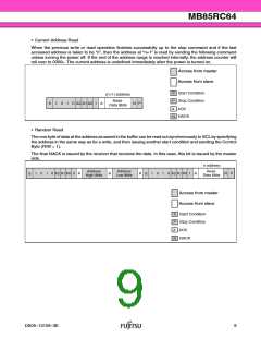
MB85RC64
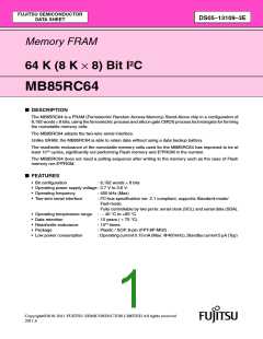
■ PIN ASSIGNMENT
(TOP VIEW)
A0
A1
1
2
3
4
8
7
6
5
VDD
WP
SCL
SDA
A2
VSS
(FPT-8P-M02)
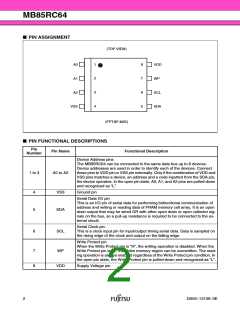
■ PIN FUNCTIONAL DESCRIPTIONS
Pin
Pin Name
Number
Functional Description
Device Address pins
The MB85RC64 can be connected to the same data bus up to 8 devices.
Device addresses are used in order to identify each of the devices. Connect
these pins to VDD pin or VSS pin externally. Only if the combination of VDD and
VSS pins matches a device, an address and a code inputted from the SDA pin,
the device operates. In the open pin state, A0, A1, and A2 pins are pulled-down
and recognized as “L”.
1 to 3
A0 to A2
4
5
VSS
SDA
Ground pin
Serial Data I/O pin
This is an I/O pin of serial data for performing bidirectional communication of
address and writing or reading data of FRAM memory cell array. It is an open
drain output that may be wired OR with other open drain or open collector sig-
nals on the bus, so a pull-up resistance is required to be connected to the ex-
ternal circuit.
Serial Clock pin
6
SCL
This is a clock input pin for input/output timing serial data. Data is sampled on
the rising edge of the clock and output on the falling edge.
Write Protect pin
When the Write Protect pin is “H”, the writing operation is disabled. When the
Write Protect pin is “L”, the entire memory region can be overwritten. The read-
ing operation is always enabled regardless of the Write Protect pin condition. In
the open pin state, the Write Protect pin is pulled-down and recognized as “L”.
7
8
WP
VDD
Supply Voltage pin
2
DS05–13109–3E

 FUJITSU [ FUJITSU ]