MB85RC64
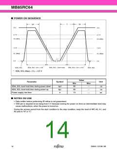
■ POWER ON SEQUENCE
tr
tpu
tpd
VCC
VCC
2.7 V
2.7 V
VIH (Min)
VIH (Min)
1.0 V
1.0 V
VIL (Max)
VIL (Max)
0 V
0 V
*
*
SDA, SCL >VCC × 0.8
SDA, SCL : Don't care
SDA, SCL >VCC × 0.8
SDA, SCL
SDA, SCL
* : SDA, SCL (Max) < VCC + 0.5 V
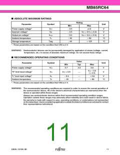
Value
Parameter
Symbol
Unit
Min
85
Max
SDA, SCL level hold time during power down
SDA, SCL level hold time during power up
Power supply rise time
tpd
tpu
tr
⎯
⎯
⎯
ns
ns
μs
85
10
■ NOTES ON USE
• Data written before performing IR reflow is not guaranteed.
• VDD pin is required to be rising from 0 V because turning the power on from an intermediate level may
cause malfunctions, when the power is turned on.
During the access period from the start condition to the stop condition, keep the level of WP, A0, A1, and
A2 pins to “H” or “L”.
14
DS05–13109–3E

 FUJITSU [ FUJITSU ]