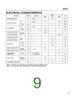
MB1507
FUNCTIONAL DESCRIPTIONS
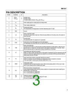
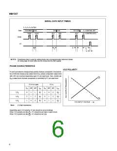
SERIAL DATA INPUT
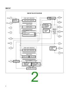
Serial data input is achieved by three inputs, such as Data pin, Clock pin and LE pin. Serial data input controls 15–bit programmable reference divider
and 19–bit programmable divider, respectively.
Binary serial data is input to Data pin.
On rising edge of clock shifts one bit of serial data into the internal shift registers and when load enable pin is high level or open, stored data is
transferred into latch depending upon the control bit.
Control data ”H” data is transferred into 15–bit latch.
Control data ”L” data is transferred into 19–bit latch.
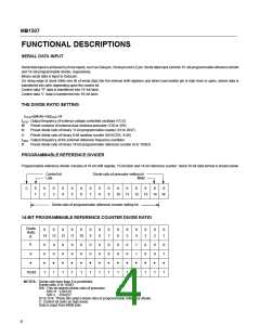
THE DIVIDE RATIO SETTING
f =[(MxN)+A]xfOSC÷R
VCO
f
M:
N:
: Output frequency of external voltage controlled oscillator (VCO)
Preset modulus of external dual modulus prescaler (128 or 256)
Preset divide ratio of binary 11-bit programmable counter (16 to 2047)
VCO
A:
Preset divide ratio of binary 8-bit swallow counter (0≤A≤255, A<N)
: Output frequency of the external reference frequency oscillator
f
OSC
R:
Preset divide ratio of binary 14-bit programmable reference counter (8 to 16383)
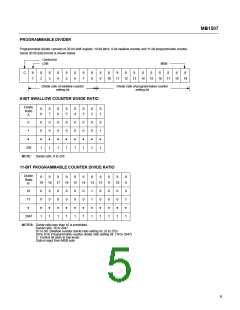
PROGRAMMABLE REFERENCE DIVIDER
Programmable reference divider consists of 16-bit shift register, 15-bit latch and 14-bit reference counter. Serial 16-bit data format is shown below.
Control bit
LSB
Divide ratio of prescaler setting bit
MSB
C
S
1
S
2
S
3
S
4
S
5
S
6
S
7
S
8
S
9
S
S
S
S
S
S
10
11
12
13
14
W
Divide ratio of programmable reference counter setting bit
14-BIT PROGRAMMABLE REFERENCE COUNTER DIVIDE RATIO
Divide
Ratio
R
S
S
S
S
S
S
9
S
8
S
7
S
6
S
5
S
4
S
3
S
2
S
1
14
13
12
11
10
8
0
0
•
0
0
•
0
0
•
0
0
•
0
0
•
0
0
•
0
0
•
0
0
•
0
0
•
0
0
•
1
1
•
0
0
•
0
0
•
0
1
•
9
•
16383
1
1
1
1
1
1
1
1
1
1
1
1
1
1
NOTES: Divide ratio less than 8 is prohibited.
Divide ratio: 8 to 16383
SW: This bit selects divide ratio of prescaler.
SW=H : 128/129
SW=L : 256/257
S1 to S14: These bits select divide ratio of programmable reference divider.
C: Control bit (sets as high level).
Data is input from MSB side.
4

 FUJITSU [ FUJITSU ]