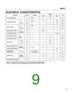
MB1507
PIN DESCRIPTION
Pin No.
Pin Name
I/O
Description
Oscillator input.
Oscillator output.
1
2
OSC
OSC
I
O
IN
OUT
A crystal is placed between OSC and OSC
.
IN
OUT
Power supply input for charge pump and analog switch.
Power supply voltage input.
3
4
V
V
P
–
–
CC
Charge pump output.
The characteristics of charge pump is reversed depending upon FC input.
5
6
D
O
–
O
Ground.
GND
LD
Phase comparator output.
Normally the output level is high level. While the phase difference of f and f exists, the output be-
7
O
r
p
comes low level.
Prescaler input.
The connection with VCO should be AC connection.
8
9
f
I
I
IN
Clock input for 20-bit shift register and 16-bit shift register.
On rising edge of the clock shifts one bit of data into the shift registers.
Clock
Binary serial data input.
The last bit of the data is a control bit which specified destination of shift registers. When this bit is
high level and LE is high level, the data stored in shift register is transferred to 15-bit latch. When
this bit is low level and LE is high level, the data is transferred to 19-bit latch.
10
11
Data
LE
I
I
Load enable input (with pull up resistor).
When LE is high or open, the data stored in shift register is transferred into latch depending upon the
control bit. At the time, internal charge pump output to be connected to BISW pin because internal
analog switch becomes ON state.
Phase select input of phase comparator (with pull up resistor).
12
13
FC
I
When FC is low level, the characteristics of charge pump, phase comparator is reversed.
FC pin input signal controls f pin (test pin) output level, f or f .
out
r
p
Analog switch output.
BISW
O
Usually BISW pin is set high-impedance state. When internal analog switch is ON (LE pin is high
level), this pin outputs internal charge pump output.
Monitor pin of phase comparator input.
f
pin outputs programmable reference divider output (f ) or programmable divider output (f ) de-
r p
out
14
f
O
pending upon FC pin input level.
FC=H: It is the same as f output level.
OUT
r
FC=L: It is the same as f output level.
p
15
16
ØP
ØR
O
O
Outputs for external charge pump.
The characteristics are reversed according to FC input.
P pin is N-channel open drain output.
3

 FUJITSU [ FUJITSU ]