FT245BL USB FIFO ( USB - Parallel ) I.C.
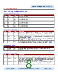
POWER CONTROL GROUP
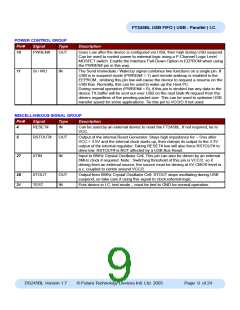
Pin#
10
Signal
Type
Description
PWREN#
OUT
Goes Low after the device is configured via USB, then high during USB suspend.
Can be used to control power to external logic using a P-Channel Logic Level
MOSFET switch. Enable the Interface Pull-Down Option in EEPROM when using
the PWREN# pin in this way.
11
SI / WU
IN
The Send Immediate / WakeUp signal combines two functions on a single pin. If
USB is in suspend mode (PWREN# = 1) and remote wakeup is enabled in the
EEPROM , strobing this pin low will cause the device to request a resume on the
USB Bus. Normally, this can be used to wake up the Host PC.
During normal operation (PWREN# = 0), if this pin is strobed low any data in the
device TX buffer will be sent out over USB on the next Bulk-IN request from the
drivers regardless of the pending packet size. This can be used to optimise USB
transfer speed for some applications. Tie this pin to VCCIO if not used.
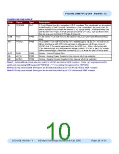
MISCELLANEOUS SIGNAL GROUP
Pin#
4
Signal
Type
Description
RESET#
IN
Can be used by an external device to reset the FT245BL. If not required, tie to
VCC.
5
RSTOUT#
XTIN
OUT
IN
Output of the internal Reset Generator. Stays high impedance for ~ 5ms after
VCC > 3.5V and the internal clock starts up, then clamps its output to the 3.3V
output of the internal regulator. Taking RESET# low will also force RSTOUT# to
drive low. RSTOUT# is NOT affected by a USB Bus Reset.
27
Input to 6MHz Crystal Oscillator Cell. This pin can also be driven by an external
6MHz clock if required. Note : Switching threshold of this pin is VCC/2, so if
driving from an external source, the source must be driving at 5V CMOS level or
a.c. coupled to centre around VCC/2.
28
31
XTOUT
TEST
OUT
IN
Output from 6MHz Crystal Oscillator Cell. XTOUT stops oscillating during USB
suspend, so take care if using this signal to clock external logic.
Puts device in I.C. test mode – must be tied to GND for normal operation.
DS245BL Version 1.7
© Future Technology Devices Intl. Ltd. 2005
Page 9 of 24

 FTDI [ FUTURE TECHNOLOGY DEVICES INTERNATIONAL LTD. ]