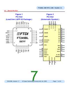
FT245BL USB FIFO ( USB - Parallel ) I.C.
4.1 Signal Descriptions
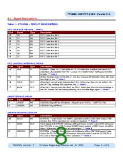
Table 1 - FT245BL - PINOUT DESCRIPTION
FIFO DATA BUS GROUP (*** Note 1)
Pin#
25
24
23
22
21
20
19
18
Signal
DO
D1
Type
I/O
I/O
I/O
I/O
I/O
I/O
I/O
I/O
Description
FIFO Data Bus Bit 0
FIFO Data Bus Bit 1
FIFO Data Bus Bit 2
FIFO Data Bus Bit 3
FIFO Data Bus Bit 4
FIFO Data Bus Bit 5
FIFO Data Bus Bit 6
FIFO Data Bus Bit 7
D2
D3
D4
D5
D6
D7
FIFO CONTROL INTERFACE GROUP
Pin#
16
Signal
Type
Description
RD#
IN
Enables Current FIFO Data Byte on D0..D7 when low. Fetches the next FIFO
Data Byte (if available) from the Receive FIFO Buffer when RD# goes from low
to high. *** Note 1
15
14
12
WR
IN
Writes the Data Byte on the D0..D7 into the Transmit FIFO Buffer when WR goes
from high to low. *** Note 1
TXE#
RXF#
OUT
OUT
When high, do not write data into the FIFO. When low, data can be written into
the FIFO by strobing WR high then low. *** Note 2
When high, do not read data from the FIFO. When low, there is data available in
the FIFO which can be read by strobing RD# low then high again *** Note 2
USB INTERFACE GROUP
Pin#
Signal
Type
I/O
Description
7
8
USBDP
USBDM
USB Data Signal Plus (Requires 1.5K pull-up to 3V3OUT or RSTOUT#)
USB Data Signal Minus
I/O
EEPROM INTERFACE GROUP
Pin#
32
Signal
Type
Description
EECS
I/O
EEPROM – Chip Select. For 48MHz operation pull EECS to GND using a 10K
resistor. For 6MHz operation no resistor is required. *** Note 3
1
2
EESK
OUT
I/O
Clock signal to EEPROM. Adding a 10K pull down resistor onto EESK will cause
the FT245BL to use USB Product ID 6005 (hex) instead of 6001 (hex). All of the
other USB device descriptors are unchanged. *** Note 3
EEDATA
EEPROM – Data I/O Connect directly to Data-In of the EEPROM and to Data-
Out of the EEPROM via a 2.2K resistor. Also pull Data-Out of the EEPROM to
VCC via a 10K resistor for correct operation. *** Note 3
DS245BL Version 1.7
© Future Technology Devices Intl. Ltd. 2005
Page 8 of 24

 FTDI [ FUTURE TECHNOLOGY DEVICES INTERNATIONAL LTD. ]