FT245BL USB FIFO ( USB - Parallel ) I.C.
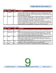
POWER AND GND GROUP
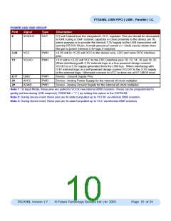
Pin#
6
Signal
Type
Description
3V3OUT
OUT
3.3 volt Output from the integrated L.D.O. regulator This pin should be decoupled
to GND using a 33nF ceramic capacitor in close proximity to the device pin. Its
prime purpose is to provide the internal 3.3V supply to the USB transceiver cell
and the RSTOUT# pin. A small amount of current (<= 5mA) can be drawn from
this pin to power external 3.3V logic if required.
3,26
13
VCC
PWR
PWR
+4.35 volt to +5.25 volt VCC to the device core, LDO and none-FIFO interface
pins.
VCCIO
+3.0 volt to +5.25 volt VCC to the FIFO interface pins 10..12, 14..16 and 18..25.
When interfacing with 3.3V external logic in a bus powered design connect
VCCIO to a 3.3V supply generated from the USB bus. When interfacing with
3.3V external logic in a self powered design connect VCCIO to the 3.3V supply
of the external logic. Otherwise connect to VCC to drive out at 5V CMOS level.
9,17
30
GND
PWR
PWR
PWR
Device - Ground Supply Pins
AVCC
AGND
Device - Analog Power Supply for the internal x8 clock multiplier
Device - Analog Ground Supply for the internal x8 clock multiplier
29
Note 1 : In Input Mode, these pins are pulled to VCCIO via internal 200K resistors. These can be programmed to
gently pull low during USB suspend ( PWREN# = “1” ) by setting this option in the EEPROM.
Note 2: During device reset, these pins are tri-state but pulled up to VCCIO via internal 200K resistors.
Note 3: During device reset, these pins are tri-state but pulled up to VCC via internal 200K resistors.
DS245BL Version 1.7
© Future Technology Devices Intl. Ltd. 2005
Page 10 of 24

 FTDI [ FUTURE TECHNOLOGY DEVICES INTERNATIONAL LTD. ]