FT245BL USB FIFO ( USB - Parallel ) I.C.
1.1 General Description
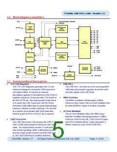
The FT245BL provides an easy cost-effective method of transferring data to / from a peripheral and a host P.C. at up
to 8 Million bits (1 Megabyte) per second. Its simple, FIFO-like design makes it easy to interface to any microcontroller
or microprocessor via IO ports.
To send data from the peripheral to the host computer, simply write the byte-wide data into the module when TXE# is
low. If the (384-byte) transmit buffer fills up or is busy storing the previously written byte, the device keeps TXE# high
in order to stop further data from being written until some of the FIFO data has been transferred over USB to the host.
TXE# goes high after every byte written.
When the host sends data to the peripheral over USB, the device will take RXF# low to let the peripheral know that at
least one byte of data is available. The peripheral can read a data byte every time RXF# goes low. RXF# goes high
after every byte read.
By using FTDI’s virtual COM port drivers, the peripheral looks like a standard COM port to the application software.
Commands to set the baud rate are ignored - the device always transfers data at its fastest rate regardless of the
application’s baud-rate setting. Alternatively, FTDI’s D2XX drivers allow application software to access the device
“directly” through a published DLL based API. Details of the current VCP and D2XX driver can be found on FTDI’s web
site ( http://www.ftdichip.com )
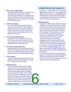
2.0 Enhancements
This section summarises the enhancements of the 2nd generation device compared to its FT8U245AM predecessor.
For further details, consult the device pin-out description and functional descriptions.
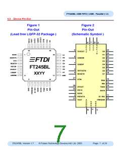
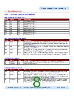
•
Integrated Power-On-Reset (POR) Circuit
The device now incorporates an internal POR
function. The existing RESET# pin is maintained
in order to allow external logic to reset the device
where required, however for many applications
this pin can now be either left N/C or hard wired
to VCC. In addition, a new reset output pin
(RSTOUT#) is provided in order to allow the new
POR circuit to provide a stable reset to external
MCU and other devices. RSTOUT# was the TEST
pin on the previous generation of devices.
•
Integrated Level Converter on FIFO interface
and control signals
The previous devices would drive the FIFO and
control signals at 5V CMOS logic levels. The
new device has a separate VCCIO pin allowing
the device to directly interface to 3.3V and other
logic families without the need for external level
converter I.C.’s
•
Power Management control for USB Bus
Powered, high current devices
•
Integrated RCCLK Circuit
A new PWREN# signal is provided which can be
used to directly drive a transistor or P-Channel
MOSFET in applications where power switching
of external circuitry is required. A new EEPROM
based option makes the device pull gently down
its FIFO interface lines when the power is shut
off (PWREN# is High). In this mode, any residual
In the previous devices, an external RC circuit
was required to ensure that the oscillator and
clock multiplier PLL frequency was stable prior
to enabling the clock internal to the device. This
circuit is now embedded on-chip – the pin assigned
to this function is now designated as the TEST pin
and should be tied to GND for normal operation.
DS245BL Version 1.7
© Future Technology Devices Intl. Ltd. 2005
Page 2 of 24

 FTDI [ FUTURE TECHNOLOGY DEVICES INTERNATIONAL LTD. ]