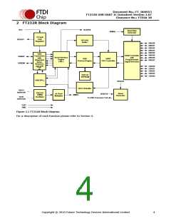
Document No.: FT_000053
FT232R USB UART IC Datasheet Version 2.07
Clearance No.: FTDI# 38
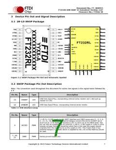
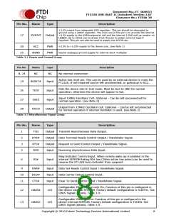
Pin No.
Name
Type
Description
+3.3V output from integrated LDO regulator. This pin should be decoupled to
ground using a 100nF capacitor. The main use of this pin is to provide the internal
+3.3V supply to the USB transceiver cell and the internal 1.5kΩ pull up resistor on
USBDP. Up to 50mA can be drawn from this pin to power external logic if
required. This pin can also be used to supply the VCCIO pin.
17
3V3OUT
Output
+3.3V to +5.25V supply to the device core. (see Note 1)
Device analogue ground supply for internal clock multiplier
20
25
VCC
PWR
PWR
AGND
Table 3.2 Power and Ground Group
Pin No.
Name
Type
Description
8, 24
NC
NC
No internal connection
Active low reset pin. This can be used by an external device to reset the
FT232R. If not required can be left unconnected, or pulled up to VCC.
19
26
27
28
RESET#
TEST
Input
Input
Puts the device into IC test mode. Must be tied to GND for normal
operation, otherwise the device will appear to fail.
Input 12MHz Oscillator Cell. Optional – Can be left unconnected for
normal operation. (see Note 2)
OSCI
Input
Output from 12MHZ Oscillator Cell. Optional – Can be left unconnected
for normal operation if internal Oscillator is used. (see Note 2)
OSCO
Output
Table 3.3 Miscellaneous Signal Group
Pin No.
Name
TXD
Type
Output
Output
Output
Input
Description
Transmit Asynchronous Data Output.
1
2
3
5
DTR#
RTS#
RXD
Data Terminal Ready Control Output / Handshake Signal.
Request to Send Control Output / Handshake Signal.
Receiving Asynchronous Data Input.
Ring Indicator Control Input. When remote wake up is enabled in the
internal EEPROM taking RI# low (20ms active low pulse) can be used to
resume the PC USB host controller from suspend.
6
RI#
Input
9
DSR#
DCD#
CTS#
Input
Input
Input
Data Set Ready Control Input / Handshake Signal.
Data Carrier Detect Control Input.
10
11
Clear To Send Control Input / Handshake Signal.
Configurable CBUS output only Pin. Function of this pin is configured in
the device internal EEPROM. Factory default configuration is SLEEP#. See
CBUS Signal Options, Table 3.9.
12
13
CBUS4
CBUS2
I/O
I/O
Configurable CBUS I/O Pin. Function of this pin is configured in the
device internal EEPROM. Factory default configuration is TXDEN. See
CBUS Signal Options, Table 3.9.
Copyright © 2010 Future Technology Devices International Limited
8

 FTDI [ FUTURE TECHNOLOGY DEVICES INTERNATIONAL LTD. ]