Document No.: FT_000053
FT232R USB UART IC Datasheet Version 2.07
Clearance No.: FTDI# 38
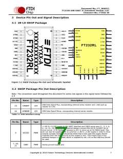
3 Device Pin Out and Signal Description
3.1 28-LD SSOP Package
4
1
VCCIO
VCC
TXD
RXD
28
TXD
1
OSCO
OSCI
20
5
DTR#
RTS#
VCCIO
RXD
16
15
USBDM
USBDP
3
TEST
RTS#
CTS#
DTR#
11
2
AGND
NC
FT232RL
8
NC
9
RI#
CBUS0
CBUS1
GND
DSR#
DCD#
RI#
19
24
RESET#
NC
GND
10
6
27
28
OSCI
NC
OSCO
DSR#
DCD#
CTS#
CBUS4
CBUS2
VCC
23
22
13
CBUS0
CBUS1
CBUS2
RESET#
GND
17
3V3OUT
A
G
N
D
T
E
S
T
3V3OUT
USBDM
USBDP
G
N
D
G
N
D
G
N
D
14
12
CBUS3
CBUS4
25
7
18
21
26
CBUS3
14
15
Figure 3.1 SSOP Package Pin Out and Schematic Symbol
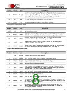
3.2 SSOP Package Pin Out Description
Note: The convention used throughout this document for active low signals is the signal name followed by
a #
Pin No.
15
Name
USBDP
USBDM
Type
I/O
Description
USB Data Signal Plus, incorporating internal series resistor and 1.5kΩ pull up
resistor to 3.3V.
USB Data Signal Minus, incorporating internal series resistor.
16
I/O
Table 3.1 USB Interface Group
Pin No.
Name
Type
Description
+1.8V to +5.25V supply to the UART Interface and CBUS group pins (1...3, 5, 6,
9...14, 22, 23). In USB bus powered designs connect this pin to 3V3OUT pin to
drive out at +3.3V levels, or connect to VCC to drive out at 5V CMOS level. This
pin can also be supplied with an external +1.8V to +2.8V supply in order to drive
outputs at lower levels. It should be noted that in this case this supply should
originate from the same source as the supply to VCC. This means that in bus
powered designs a regulator which is supplied by the +5V on the USB bus should
be used.
4
VCCIO
PWR
7, 18,
21
Device ground supply pins
GND
PWR
Copyright © 2010 Future Technology Devices International Limited
7

 FTDI [ FUTURE TECHNOLOGY DEVICES INTERNATIONAL LTD. ]