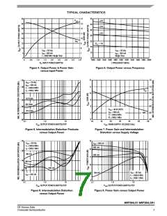
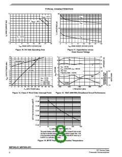
TYPICAL CHARACTERISTICS
3
2
100
T
= 75°C
flange
C
iss
T
= 100°C
flange
C
oss
10
1
0
T = 175°C
C
J
rss
1
0
4
8
12
16
20
24
28
0
4
8
12
V , DRAIN SOURCE VOLTAGE (VOLTS)
DS
16
20
24
28
V
, DRAIN SUPPLY VOLTAGE (Vdc)
DD
Figure 10. DC Safe Operating Area
Figure 11. Capacitance versus
Drain Source Voltage
60
50
40
30
11
10
9
45
G
ps
40
FUNDAMENTAL
35
20
10
η
V
= 26 Vdc
DD
out
8
30
0
P
= 30 W (PEP), I = 200 mA
DQ
−10
−ꢁ20
−ꢁ30
−ꢀ40
−ꢀ50
−ꢁ60
−70
−ꢁ80
−ꢁ90
3rd Order
Two−Tone
Frequency Delta = 100 kHz
3.0
2.0
7
−32
6
IMD
V
= 26 Vdc
= 1.8 Adc
5
−36
−40
DD
I
DQ
f = 2000.0 MHz
4
3
1
VSWR
f = 2000.1 MHz
2
1.0
0
5
10 15 20 25 30 35 40 45 50 55 60
P , INPUT POWER (dBm)
1920
1940
1960
1980
2000
f, FREQUENCY (MHz)
in
Figure 12. Class A Third Order Intercept Point
Figure 13. 1920-2000 MHz Broadband Circuit Performance
1.E+10
1.E+09
1.E+08
1.E+07
1.E+06
1.E+05
1.E+04
0
50
100
150
200
250
T , JUNCTION TEMPERATURE (°C)
J
2
This graph displays calculated MTTF in hours x ampere drain current.
Life tests at elevated temperature have correlated to better than 10%
2
of the theoretical prediction for metal failure. Divide MTTF factor by I
for MTTF in a particular application.
D
Figure 14. MTTF Factor versus Junction Temperature
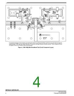
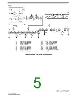
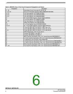
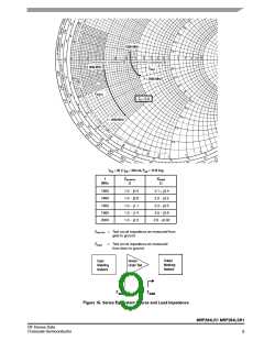
MRF284LR1 MRF284LSR1
RF Device Data
Freescale Semiconductor
8

 FREESCALE [ Freescale ]