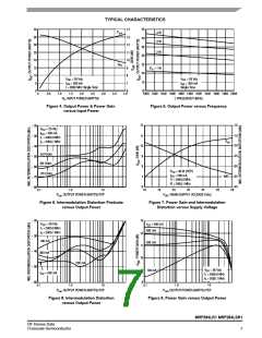
TYPICAL CHARACTERISTICS
14
13
12
11
10
9
40
35
30
25
20
15
10
5
45
40
35
30
25
20
15
10
P
4 W
3 W
out
2 W
G
ps
P
= 1 W
in
8
V
I
= 26 Vdc
= 200 mA
V
I
= 26 Vdc
DD
= 200 mA
DD
7
DQ
DQ
f = 2000 MHz Single Tone
1.5 2.0 2.5
P , INPUT POWER (WATTS)
Single Tone
6
4.0
0
0
0.5
1.0
3.0
3.5
1800 1820 1840 1860 1880 1900 1920 1940 1960 1980 2000
f, FREQUENCY (MHz)
in
Figure 4. Output Power & Power Gain
versus Input Power
Figure 5. Output Power versus Frequency
12
−10
−ꢀ20
−ꢀ30
−ꢀ40
−ꢀ50
−ꢀ60
−ꢀ70
−ꢀ80
V
= 26 Vdc
= 200 mA
DD
I
DQ
f = 2000.0 MHz
−15
−20
11
10
1
G
ps
f = 2000.1 MHz
2
3rd Order
5th Order
−25
−30
9
8
7
6
P
= 30 W (PEP)
= 200 mA
out
7th Order
I
DQ
IMD −35
f1 = 2000.0 MHz
f2 = 2000.1 MHz
−40
28
0.1
1.0
10
16
18
20
V , DRAIN SUPPLY VOLTAGE (Vdc)
DD
22
24
26
P
, OUTPUT POWER (WATTS) PEP
out
Figure 6. Intermodulation Distortion Products
versus Output Power
Figure 7. Power Gain and Intermodulation
Distortion versus Supply Voltage
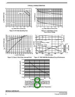
−ꢀ20
−ꢀ30
−ꢀ40
−ꢀ50
−ꢀ60
13
V
= 26 Vdc
f = 2000.0 MHz
I
= 400 mA
DD
DQ
1
f = 2000.1 MHz
300 mA
2
12
11
10
9
100 mA
300 mA
200 mA
200 mA
V
= 26 Vdc
f = 2000.0 MHz
100 mA
DD
I
= 400 mA
DQ
1
f = 2000.1 MHz
2
8
0.1
0.1
1.0
10
1.0
10
P
, OUTPUT POWER (WATTS) PEP
P , OUTPUT POWER (WATTS) PEP
out
out
Figure 8. Intermodulation Distortion
versus Output Power
Figure 9. Power Gain versus Output Power
MRF284LR1 MRF284LSR1
RF Device Data
Freescale Semiconductor
7

 FREESCALE [ Freescale ]