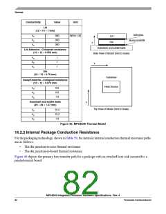
Thermal
Conductivity
Value
Unit
Lid
(12 × 14 × 1 mm)
Adhesive
kx
ky
kz
360
360
360
W/(m × K)
Lid
Bump/underfill
Die
z
Substrate and solder balls
Lid Adhesive—Collapsed resistance
(10 × 12 × 0.050 mm)
Side View of Model (Not to Scale)
kx
ky
kz
1
1
1
x
Die
(10 × 12 × 0.76 mm)
Substrate
Bump/Underfill—Collapsed resistance
(10 × 12 × 0.070 mm)
Heat Source
kx
ky
kz
0.6
0.6
1.9
Substrate and Solder Balls
y
(29 × 29 × 1.47 mm)
Top View of Model (Not to Scale)
kx
ky
kz
10.2
10.2
1.6
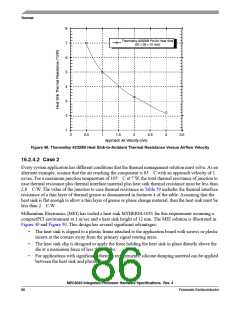
Figure 45. MPC8540 Thermal Model
16.2.2 Internal Package Conduction Resistance
For the packaging technology, shown in Table 59, the intrinsic internal conduction thermal resistance paths
are as follows:
•
•
The die junction-to-case thermal resistance
The die junction-to-board thermal resistance
Figure 46 depicts the primary heat transfer path for a package with an attached heat sink mounted to a
printed-circuit board.
MPC8540 Integrated Processor Hardware Specifications, Rev. 4
82
Freescale Semiconductor

 FREESCALE [ Freescale ]