Freescale Semiconductor, Inc.
SECTION 3 CENTRAL PROCESSING UNIT
This section presents information on M68HC11 central processing unit (CPU) archi-
tecture. Data types, addressing modes, the instruction set, and the extended address-
ing range required to support this MCU’s memory expansion feature are also included,
as are special operations such as subroutine calls and interrupts.
The CPU is designed to treat all peripheral, I/O, and memory locations identically as
addresses in the 64 Kbyte memory map. This is referred to as memory-mapped I/O.
There are no special instructions for I/O that are separate from those used for memory.
This architecture also allows accessing an operand from an external memory location
with no execution-time penalty.
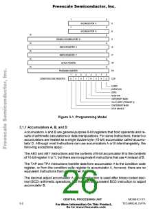
3.1 CPU Registers
M68HC11 CPU registers are an integral part of the CPU and are not addressed as if
they were memory locations. The seven registers, discussed in the following para-
graphs, are shown in Figure 3-1.
CENTRAL PROCESSING UNIT
TECHNICAL DATA
3-1
For More Information On This Product,
Go to: www.freescale.com

 FREESCALE [ Freescale ]